

Printed gas-guiding board
A technology of air guide plate and substrate, which is applied in the direction of printed circuit, printed circuit manufacturing, electrical components, etc. It can solve the problems of lack of support points, air guide plate falling off, etc., and achieve good air guide effect
- Summary
- Abstract
- Description
- Claims
- Application Information
AI Technical Summary
Problems solved by technology
Method used
Image


Examples
Embodiment
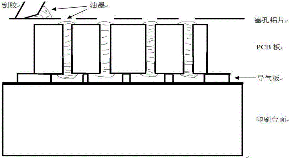
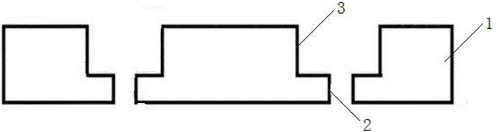
[0017] refer to image 3 , a printed air guide plate, including a substrate 1, the substrate 1 is provided with a borehole through the substrate, the borehole is composed of a first borehole 2 and a second borehole 3, the second borehole 2 Located above the first borehole 3 , and the second borehole 2 communicates with the first borehole 3 .
[0018] In this embodiment, the drilled holes penetrating the substrate are in an inverted "convex" shape.
[0019] In this embodiment, the thickness of the substrate 1 is 2.0mm.
[0020] In this embodiment, the diameter of the first borehole 2 is 0.4mm.
[0021] In this embodiment, the drilling depth of the second drilling 3 is 1.2mm, and the diameter is 2.0mm (ensure that the diameter of the hole is 1.0mm larger than that of the plug hole to prevent the ink from sticking to the air guiding plate).
[0022] Its production method: use a 2.0mm substrate as the carrier, use a 0.4mm drill bit to drill through, and use 2.0mm at the positio...
PUM
 Abstract
Description
Claims
Application Information