Voltage sampling circuit
A sampling circuit and voltage sampling technology, which is applied in the direction of measuring current/voltage, measuring electrical variables, measuring devices, etc., can solve the problems of output voltage jitter, complex circuits, and many components, and achieve high stability and reliability. The effect of small circuit loss and simple sampling circuit
- Summary
- Abstract
- Description
- Claims
- Application Information
AI Technical Summary
Problems solved by technology
Method used
Image

Examples
no. 1 example
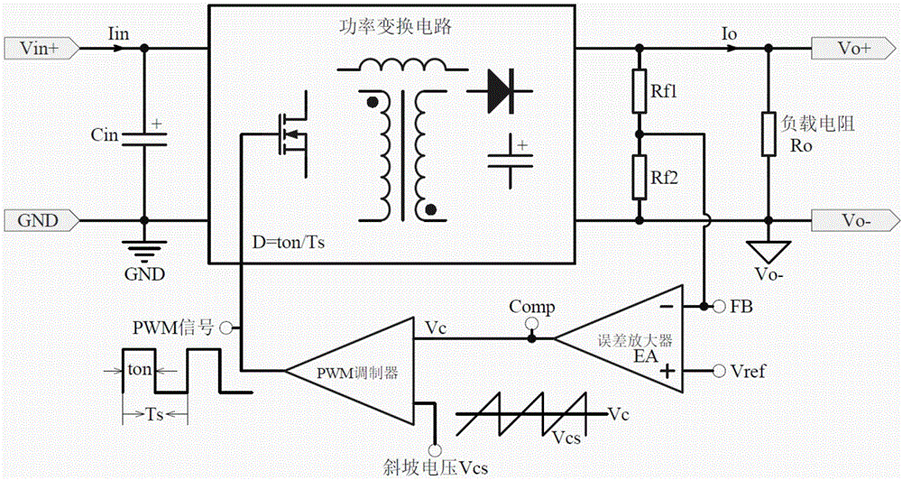
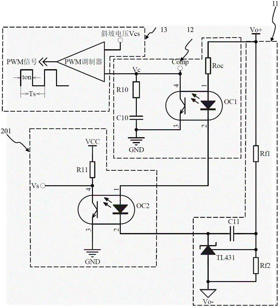
[0033] diagram 2-1 Shows the schematic circuit diagram of the first embodiment of the present invention, 11 is the output voltage sampling circuit, 12 is the optocoupler transmission circuit, 13 is the PWM modulation circuit, 201 is the optocoupler sampling circuit.
[0034] The output voltage sampling circuit includes a first sampling resistor Rf1, a second sampling resistor Rf2, a second compensation capacitor C11 and an adjustable voltage regulator TL431; the optocoupler transmission circuit includes an optocoupler current-limiting resistor Roc, a first optocoupler OC1, a first optocoupler The compensation resistor R10 and the first compensation capacitor C10; the PWM modulation circuit includes a PWM modulator and a ramp voltage Vcs; the optocoupler sampling circuit includes a power supply VCC, the second optocoupler OC2 and the first resistor R11; the first sampling resistor Rf1 The pin is connected to the positive output pole Vo+ of the switching converter, and the seco...
no. 2 example
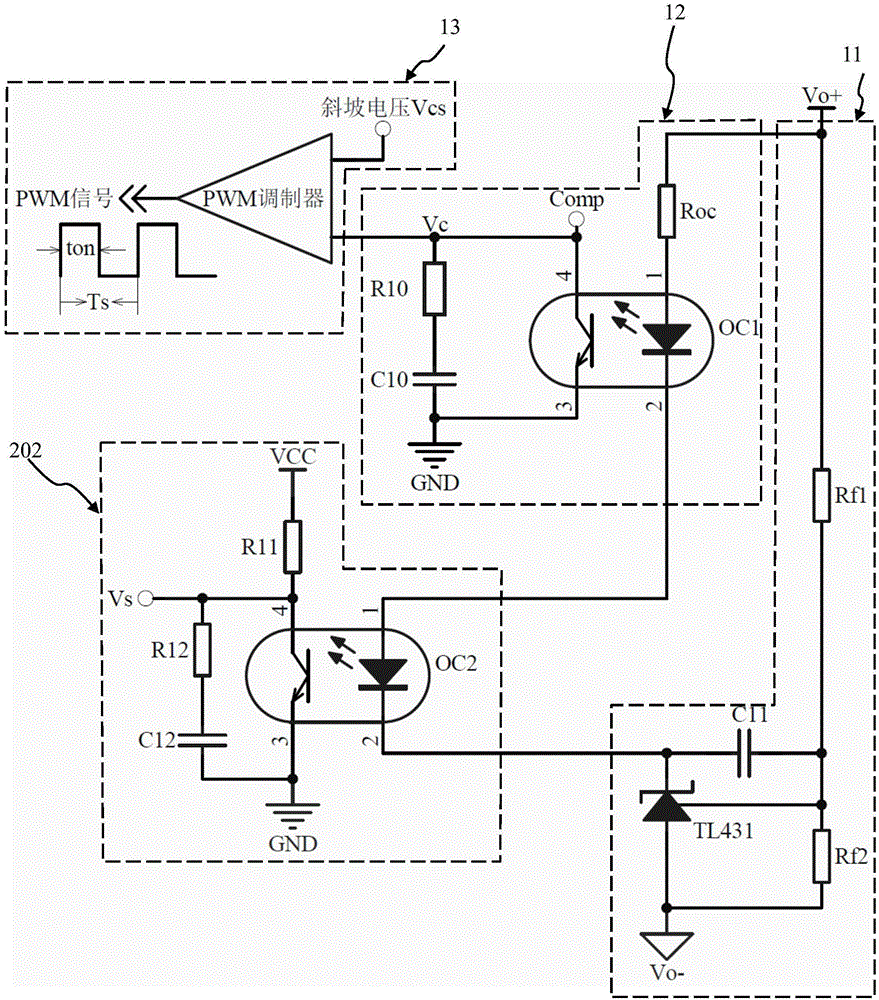
[0039] Figure 2-2 shows the circuit schematic diagram of the second embodiment of the present invention, and diagram 2-1 Compared to the circuit shown, the Figure 2-2 The difference of the circuit shown is that the second resistor R12 and the first capacitor C12 are added; R12 and C12 are connected in series, the first pin of R12 is connected with the fourth pin of OC2 and the second pin of R11, and the The second pin is connected to the first pin of C12, and the second pin of C12 and the third pin of OC2 are connected to the input ground GND; the fourth pin of the second optocoupler OC2 (or the first pin of R12) As the output terminal of the voltage sampling circuit of the present invention, the sampling voltage Vs is output. The effect of adding R12 and C12 is to make the whole voltage sampling circuit easier to debug and work stably. Figure 2-2 The circuit shown with diagram 2-1 The working principles of the circuits shown are basically the same, and the implementa...
no. 3 example
[0041] Figure 2-3 shows the schematic diagram of the circuit of the third embodiment of the present invention, and Figure 2-2 The difference of the circuit shown is that the sampling point is changed from the first pin of the second resistor R12 to the second pin of R12 to output the sampling voltage Vs, Vs is equal to the voltage Vc12 at both ends of the first capacitor C12, and is compatible with the light The voltage V43 between the fourth pin of the coupling OC2 and GND is basically equal, that is, Vs=Vc12≈V43. After changing the sampling point, the sampling voltage Vs is more "clean", carries less clutter, and the sampling voltage is more stable.
PUM
 Abstract
Description
Claims
Application Information
 - R&D
- Intellectual Property
- Life Sciences
- Materials
- Tech Scout
- Unparalleled Data Quality
- Higher Quality Content
- 60% Fewer Hallucinations
Browse by: Latest US Patents, China's latest patents, Technical Efficacy Thesaurus, Application Domain, Technology Topic, Popular Technical Reports.
© 2025 PatSnap. All rights reserved.Legal|Privacy policy|Modern Slavery Act Transparency Statement|Sitemap|About US| Contact US: help@patsnap.com