Array substrate and manufacturing method thereof

A technology of an array substrate and a manufacturing method, applied in the field of liquid crystal display, can solve the problems of poor uniformity of PI film thickness and uneven display brightness, and achieve the effect of improving uniformity and avoiding mura

Active Publication Date: 2019-08-30
TCL CHINA STAR OPTOELECTRONICS TECH CO LTD
View PDF3 Cites 0 Cited by
  • Summary
  • Abstract
  • Description
  • Claims
  • Application Information

AI Technical Summary

Problems solved by technology

[0003] However, in the subsequent manufacture of PI film (Polyimide Film, polyimide film or guide film), the PI film is solidified by the flow and diffusion of the PI solution, and the uniformity of the thickness of the PI film depends entirely on the flow and diffusion of the PI solution. , because the effective display area 11 is surrounded by the color-resist layer 12, the PI solution cannot continue to diffuse outward due to the blocking of the color-resist layer 12, so that the thickness of the PI film at the position in contact with the color-resist layer 12 is relatively large, resulting in the effective display area 11 The uniformity of the thickness of the PI film at the edge is poor, and the phenomenon of mura (uneven display brightness) will appear here

Method used


Image

  • Array substrate and manufacturing method thereof
  • Array substrate and manufacturing method thereof
  • Array substrate and manufacturing method thereof

Examples


Embodiment Construction

[0023] The following will clearly and completely describe the technical solutions of each exemplary embodiment provided by the present invention with reference to the accompanying drawings in the embodiments of the present invention. In the case of no conflict, the following embodiments and features in the embodiments can be combined with each other. Moreover, the directional terms used throughout the present invention, such as "upper" and "lower", are all for better describing various embodiments, and are not used to limit the protection scope of the present invention.

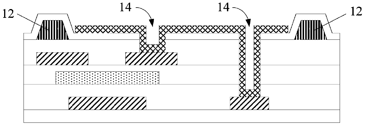
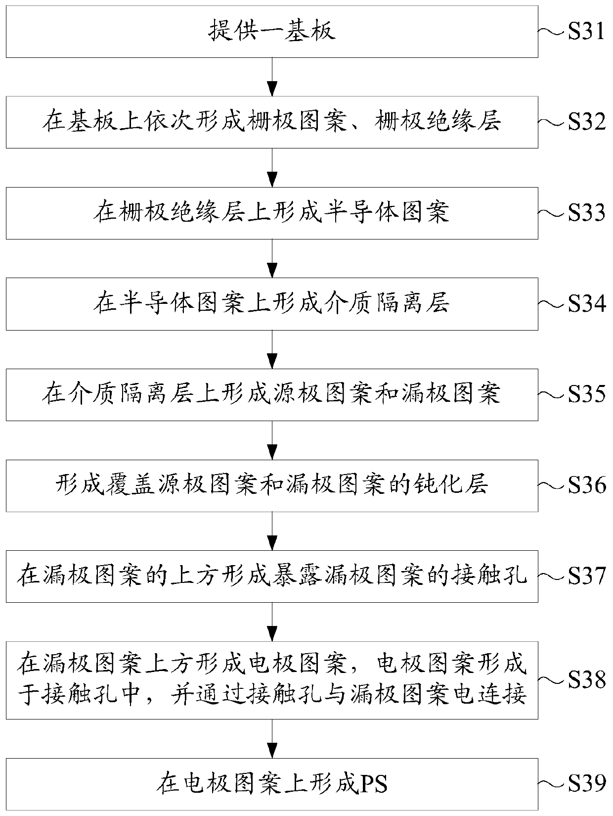
[0024] see image 3 and Figure 4 , is a method for manufacturing an array substrate according to an embodiment of the present invention. The manufacturing method of the array substrate may include steps S31-S39.

[0025] S31: Provide a substrate.

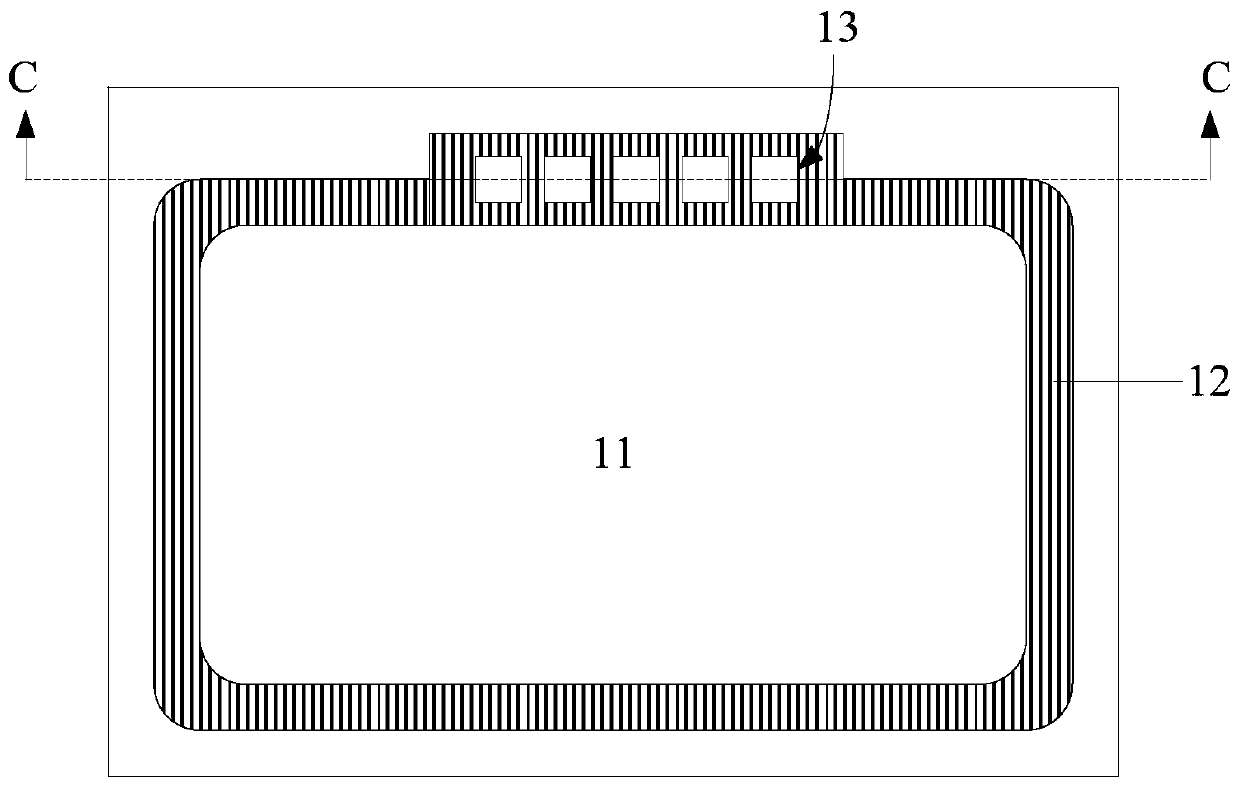
[0026] Such as Figure 4 As shown, the substrate 41 includes but not limited to glass substrates, transparent plastic substrates and flexible substrates. Ce...


PUM


Abstract

The invention discloses an array substrate and a manufacturing method thereof. The manufacturing method comprises the steps of: forming a thin film transistor in a non-display region of a substrate, which corresponds to the array substrate; forming a via hole for exposing a drain electrode pattern above the drain electrode pattern; forming an electrode pattern above the thin film transistor, wherein the electrode pattern is formed in the via hole and is electrically connected with the drain electrode pattern by the via hole; and forming a PS (Photo Spacer) on the electrode pattern. According to the array substrate and the manufacturing method thereof, which are disclosed by the invention, uniformity of a thickness of a PI film at the edge of an effective display region can be improved, a mura phenomenon at the edge of the effective display region is avoided, and a contact impedance of the electrode pattern can be reduced.

Description

technical field [0001] The invention relates to the field of liquid crystal display, in particular to an array substrate and a manufacturing method thereof. Background technique [0002] In order to prevent the ITO (Indium tin oxide, indium tin oxide or transparent electrode) separately arranged on the array substrate and the color filter substrate from contacting and short circuiting to cause signal abnormalities, such as figure 1 and figure 2 As shown, a color-resist layer 12 of a predetermined height, such as a blue color-resist layer, is provided around the active area (ActiveArea, AA) 11 of the liquid crystal display panel, and the purpose of supporting the two substrates is achieved through the color-resist layer 12 . Wherein, the color resist layer 12 surrounds the traces of the fanout 13 of the liquid crystal display panel, that is, is arranged around the contact hole (Via hole) 14 of the fanout 13 . [0003] However, in the subsequent manufacture of PI film (Poly...

Claims


Application Information

Patent Timeline
Patent Type & Authority Patents(China)
IPC IPC(8): H01L21/84H01L27/12
Inventor 王金杰王笑笑
Owner TCL CHINA STAR OPTOELECTRONICS TECH CO LTD
Why Eureka
Try Eureka