Supercharge Your Innovation With Domain-Expert AI Agents!

A Thin Film Transistor with High Effective Power

A thin film transistor and semiconductor technology, applied in transistors, semiconductor devices, electrical components, etc., can solve problems such as large power consumption, and achieve the effects of reducing power consumption, increasing area, and improving effective power

Active Publication Date: 2019-08-02
上海禾馥电子有限公司
View PDF4 Cites 0 Cited by
  • Summary
  • Abstract
  • Description
  • Claims
  • Application Information

AI Technical Summary

Problems solved by technology

[0004] In order to form a good contact between the semiconductor layer and the source-drain, an ohmic contact layer with N-type doping or P-type doping is usually formed on the semiconductor layer, which reduces the contact between the semiconductor layer and the source to a certain extent. electrode, or the contact resistance between the semiconductor layer and the drain, even so, the power consumption caused by the metal-semiconductor contact is still relatively large, and the improvement of power consumption still needs to be improved

Method used


Image

  • A Thin Film Transistor with High Effective Power
  • A Thin Film Transistor with High Effective Power
  • A Thin Film Transistor with High Effective Power

Examples


Embodiment 1

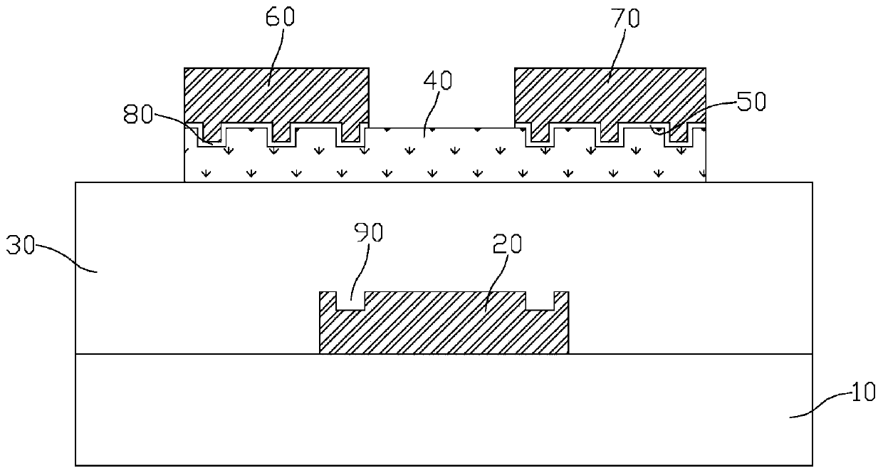
[0028] See figure 1 As shown, a thin film transistor with high effective power includes: a substrate 10, a gate 20 disposed on the substrate 10, a gate insulating layer 30 disposed on the substrate 10 and covering the gate 20, and a gate insulating layer 30 on the surface of the gate insulating layer 30. The semiconductor layer 40, and the source level 60 and the drain level 70 arranged on the semiconductor layer 40, and the source electrode 60 is arranged opposite to the drain electrode 70, and the upper surface of the semiconductor layer 40 forms several first The groove 80, the ohmic contact layer 50 is formed on the projection of the source electrode 60 and the drain electrode 70 on the upper surface of the semiconductor layer 40, the shape of the ohmic contact layer 50 changes with the shape of the upper surface of the semiconductor layer 40, and the source electrode 60 and the drain electrode 70 are formed On the ohmic contact layer 50, when the first groove 80 forms a p...

Embodiment 2

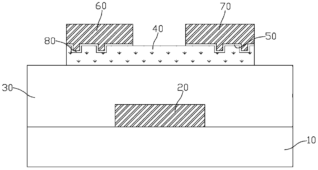
[0033] See figure 2 As shown, in this embodiment, four first grooves 80 are formed on the upper surface of the semiconductor layer 40, two of which are formed at the projection of the source 60, and two are formed at the projection of the source and drain 70. The first groove 80 does not form a projection at the gate 20, and there is no need to form a second groove 90 on the upper surface of the gate 20, which can simplify the manufacturing process, and the rest of the structural configuration is the same as that of Embodiment 1.

Embodiment 3

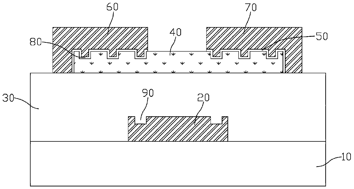
[0035] See image 3 As shown, in this embodiment, the ohmic contact layer 50 is also formed on both sides of the semiconductor layer 40, and the source electrode 20 and the drain electrode 70 extend on both sides of the ohmic contact layer 50, wrapping the two sides of the ohmic contact layer 50, further increasing the metal The semiconductor contact area reduces power consumption, and the rest of the structural configuration is the same as that of Embodiment 1.


PUM


Abstract

The invention discloses a thin film transistor with high effective power, comprising a substrate, a gate electrode arranged on the substrate, a gate insulating layer which is arranged on the substrate and covers a gate electrode, a semiconductor layer on the surface of the gate insulating layer, and a source electrode and a drain electrode which are arranged on the semiconductor layer, wherein the source electrode is arranged opposite to the drain electrode, the upper surface of the semiconductor layer forms a plurality of first grooves at the projection part of the source electrode and the drain electrode, an ohmic contact layer is formed at the projection part of the source electrode and the drain electrode on the upper surface of the semiconductor layer, the shape of the ohmic contact layer changes with the shape of the upper surface of the semiconductor layer, the source electrode and the drain electrode are formed on the ohmic contact layer, the upper surface of the gate electrode forms a second groove in a corresponding projection area when the first groove forms projection at the gate electrode, and the shape and dimension of the second groove is the same as the corresponding first groove. According to the thin film transistor with high effective power disclosed by the invention, the power consumption caused by the contact between semiconductors and the source and drain metal can be further reduced, and the effective power of the thin film transistor can be increased.

Description

technical field [0001] The invention relates to the technical field of semiconductors, in particular to a thin film transistor. Background technique [0002] Thin-film transistors are widely used as switching devices for each pixel of a display device such as an LCD. Generally speaking, a thin-film transistor has at least a gate, a source, a drain, and a semiconductor layer. The semiconductor layer can be changed by controlling the voltage of the gate. The conductivity of the layer, so that the state of conduction (open) or insulation (closed) is formed between the source and the drain. [0003] The current-voltage properties of thin film transistors commonly used in display devices are affected by factors such as the characteristics of the semiconductor layer and the gate insulating layer in the thin film transistor, the interface properties between the gate insulating layer and the semiconductor layer, field-effect electron mobility, and the characteristics of the thin fil...

Claims


Application Information

Patent Timeline
Patent Type & Authority Patents(China)
IPC IPC(8): H01L29/417H01L29/423H01L29/786
CPCH01L29/41733H01L29/42384H01L29/7869
Inventor 李风浪李舒歆
Owner 上海禾馥电子有限公司
Features
  • R&D
  • Intellectual Property
  • Life Sciences
  • Materials
  • Tech Scout
  • Unparalleled Data Quality
  • Higher Quality Content
  • 60% Fewer Hallucinations
Learn More