

Method of forming semiconductor device
A semiconductor and device technology, applied in the field of semiconductor device formation, can solve problems such as poor performance of semiconductor devices, achieve the effects of lower precision requirements, enhanced protection, and improved performance
- Summary
- Abstract
- Description
- Claims
- Application Information
AI Technical Summary
Problems solved by technology
Method used
Image

Examples
Embodiment Construction
[0023] As mentioned in the background, semiconductor devices formed in the prior art have poor performance.
[0024] figure 1 , Figure 2a , Figure 2b , Figure 3a , Figure 3b , Figure 4a , Figure 4b , Figure 5a , Figure 5b , Figure 6a with Figure 6b It is a structural schematic diagram of the process of forming a semiconductor device in the prior art.
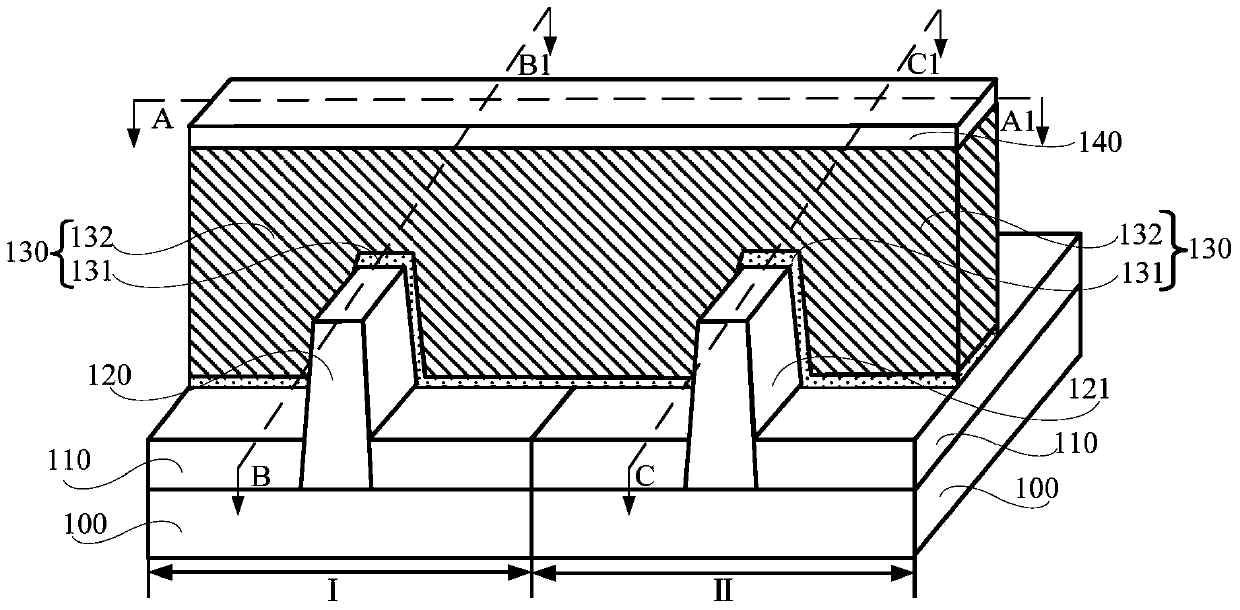
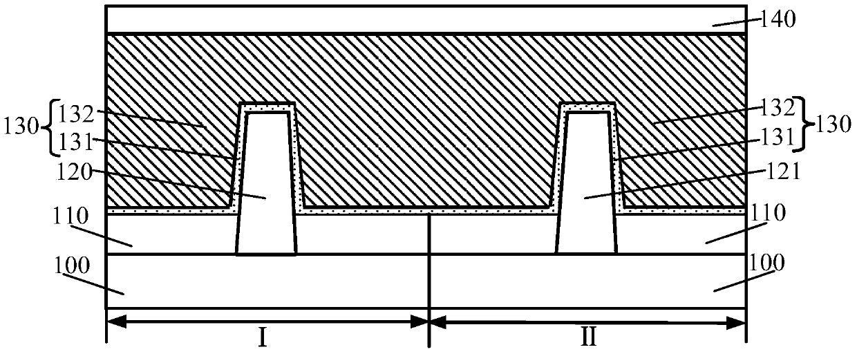
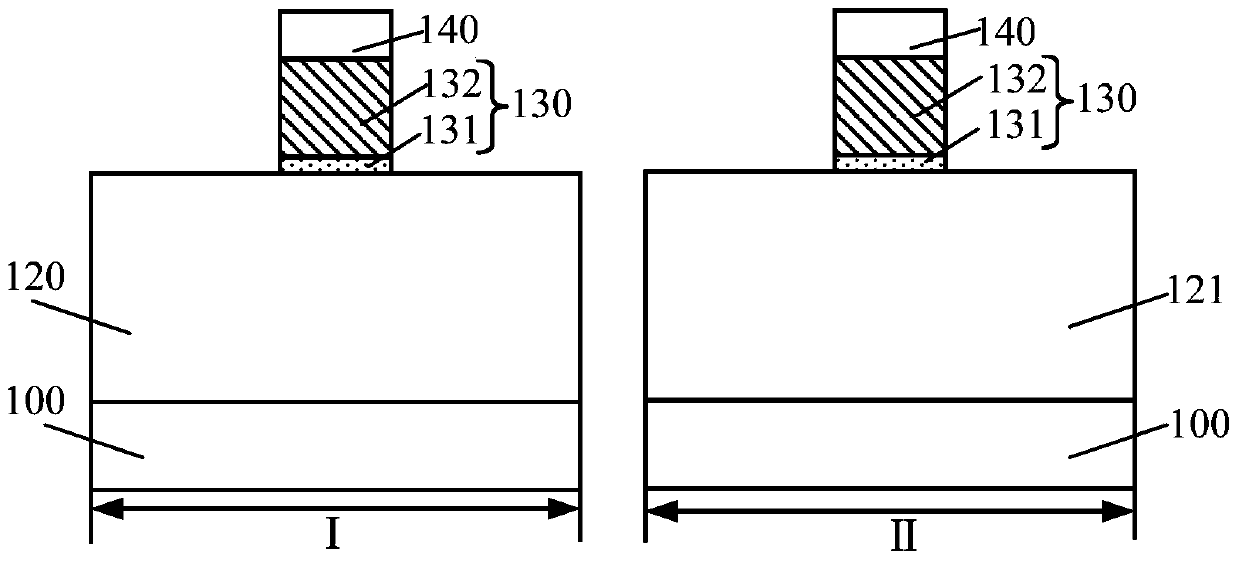
[0025] combined reference figure 1 , Figure 2a with Figure 2b , Figure 2a for along figure 1 Sectional view obtained by cutting line A-A1 in the middle, Figure 2b for along figure 1 The cross-sectional view obtained by cutting lines B-B1 and C-C1 provides a semiconductor substrate 100, the semiconductor substrate 100 has an adjacent first region (I region) and a second region (II region), and the semiconductor substrate of the I region The surface of the bottom 100 has a first fin 120, the surface of the semiconductor substrate 100 in the II region has a second fin 121, and the surface of the semic...
PUM
 Abstract
Description
Claims
Application Information