Test system and test method for testing semiconductor laser

A test method and test system technology, applied in the direction of testing optical performance, etc., can solve the problems that the production process cannot be effectively controlled, the inspection cycle is long, and the cost is high, so as to protect the interests of customers, reduce the cost of inspection, and reduce the cost of products. Effect

Inactive Publication Date: 2017-05-10
江苏飞格光电有限公司
View PDF0 Cites 4 Cited by
  • Summary
  • Abstract
  • Description
  • Claims
  • Application Information

AI Technical Summary

Problems solved by technology

Among them, in the prior art, the testing method of the optical power stability of the device working in the high and low temperature environment has always been based on the high-end chip screening method and the sample delivery test of the client terminal. Traditionally, such testing will cause many errors. The determined influencing factors make the production process unable to be effectively controlled, and there are also problems such as long inspection cycle and high cost

Method used


Image

  • Test system and test method for testing semiconductor laser

Examples


Embodiment Construction

[0017] The semiconductor laser testing system of the present invention will be further described in detail below in conjunction with the accompanying drawings and specific embodiments.

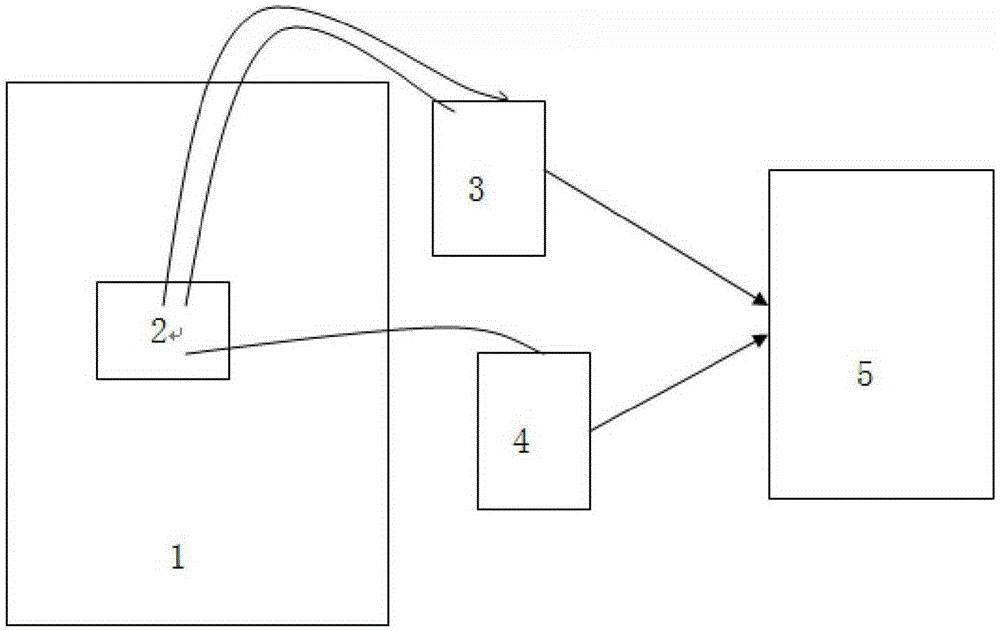
[0018] As shown in the figure, the semiconductor laser testing system of the present invention is characterized in that it includes an optical device to be tested 2 and a high and low temperature cycle box 1 for placing the optical device to be tested (laser) 2, the optical device to be tested 2 and a A current source 3 capable of providing current to the optical device 2 to be tested is connected, and the optical device 2 to be tested is also connected to an optical power meter 4 capable of testing its output optical power, and the output signal terminals of the current source 3 and the optical power meter 4 are connected to a on computer 5.

[0019] The high and low temperature working environment referred to in the test method of the test system of the semiconductor laser in this embodiment...


PUM


Abstract

The present invention discloses a working performance detecting technology for a semiconductor laser, and particularly relates to a test system and a test method for testing the semiconductor laser, which belong to the technical field of semiconductor photoelectric device manufacturing technology. The system comprises a to-be-tested optical device and a high and low temperature circulation box used for placing the to-be-tested optical device. The to-be-tested optical device is connected with a current source used for supplying a current source to the to-be-tested optical device. The to-be-tested optical device is also connected with an optical power meter used for testing the output optical power. The current source and the output signal end of the optical power meter are connected with a computer. Based on the above structure and the above method, the detection can be conveniently, effectively and quickly conducted. The working stability and the failure mode of a laser are pre-determined, so that the detection period is greatly shortened. The detection cost is greatly reduced. Meanwhile, the production process is effectively controlled and the product cost is reduced to a minimum value. Simultaneously, the benefits of customers are ensured. The test method is simple and convenient. The construction cost of the test system is low.

Description

technical field [0001] The invention relates to a working performance detection technology of a semiconductor laser, in particular to a testing system and a testing method of a semiconductor laser, belonging to the technical field of semiconductor photoelectric device manufacturing. Background technique [0002] With the rapid development of semiconductor optoelectronic device manufacturing technology, the reliability requirements of optical devices are getting higher and higher, so it is very necessary to test the reliability of devices in the production process. Among them, in the prior art, the testing method of the optical power stability of the device working in the high and low temperature environment has always been based on the high-end chip screening method and the sample delivery test of the client terminal. Traditionally, such testing will cause many errors. The determined influencing factors make the production process unable to be effectively controlled, and the...

Claims


Application Information

Patent Timeline
IPC IPC(8): G01M11/02
Inventor 詹敦平方文银
Owner 江苏飞格光电有限公司
Why Eureka
Try Eureka