Array substrate, liquid crystal display panel and touch display device

An array substrate, touch electrode technology, applied in optics, instruments, electrical and digital data processing, etc., can solve problems such as short circuits

Active Publication Date: 2017-05-10
XIAMEN TIANMA MICRO ELECTRONICS
View PDF4 Cites 16 Cited by
  • Summary
  • Abstract
  • Description
  • Claims
  • Application Information

AI Technical Summary

Problems solved by technology

[0004] The present invention provides an array substrate, a liquid crystal display panel, and a touch display device to solve the problem of short circuit between the bridge structure of the pixel electrode...

Method used


Image

  • Array substrate, liquid crystal display panel and touch display device
  • Array substrate, liquid crystal display panel and touch display device
  • Array substrate, liquid crystal display panel and touch display device

Examples


Embodiment Construction

[0022] The present invention will be further described in detail below in conjunction with the accompanying drawings and embodiments. It should be understood that the specific embodiments described here are only used to explain the present invention, but not to limit the present invention. In addition, it should be noted that, for the convenience of description, only some structures related to the present invention are shown in the drawings but not all structures. Throughout this specification, the same or similar reference numerals represent the same or similar structures, elements or processes. It should be noted that, in the case of no conflict, the embodiments in the present application and the features in the embodiments can be combined with each other.

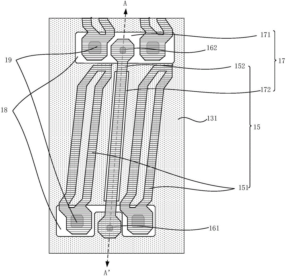
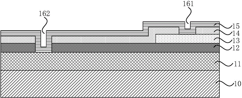
[0023] An embodiment of the present invention provides an array substrate, including a base substrate, a touch wiring layer, a first insulating layer, a touch electrode layer, a second insulating layer, and a pixel elec...


PUM


Abstract

The present invention discloses an array substrate, a liquid crystal display panel and a touch display device. The array substrate comprises: a base substrate, as well as a touch trace layer including a plurality of touch traces, a first insulating layer, touch electrode layer including a plurality of touch electrode blocks in matrix arrangement, a second insulating layer, and a pixel electrode layer including a plurality of pixel electrodes in matrix arrangement and a bridge structure, which are disposed on the base substrate in sequence, wherein the touch traces are electrically connected to the corresponding touch electrode blocks by means of the bridge structure; the bridge structure fills up and runs through first via holes of the second insulating layer that expose the touch electrode blocks and run through second via holes of the second insulating layer and the first insulating layer that expose the traces; and the bridge structure is located between every two adjacent columns of pixel electrodes, and the first via holes and the second via holes that the bridge structure correspondingly fills up are spaced apart by at least one row of pixel electrodes. With the technical solution provided in the present invention, risks of short-circuiting between the bridge structure and the pixel electors are reduced, and the yield of manufacturing of liquid crystal display panels is improved.

Description

technical field [0001] The embodiments of the present invention relate to the field of touch technology, and in particular, to an array substrate, a liquid crystal display panel and a touch display device. Background technique [0002] At present, the touch wires in the touch display device need to be electrically connected to the touch electrode blocks corresponding to the touch electrode layer. Generally, the pixel electrode layer is used to bridge the touch wires and the corresponding touch electrode blocks. Specifically, The implementation method is to use the pixel electrode layer to form a cross-bridge structure. The bridge structure connects each touch electrode block with the touch trace through the shallow hole extending to the touch electrode layer and the deep hole extending to the touch trace layer. The touch traces corresponding to the layers are electrically connected. Generally corresponding to each touch electrode block, the deep holes and shallow holes corr...

Claims


Application Information

Patent Timeline
IPC IPC(8): G02F1/1362G02F1/1343G02F1/1333G06F3/041
CPCG02F1/13338G02F1/134309G02F1/136286G06F3/0412G06F3/0416
Inventor 刘婵张磊
Owner XIAMEN TIANMA MICRO ELECTRONICS
Why Eureka
Try Eureka