Preparation method of laminated magnetic bead

A multi-layer chip and magnetic bead technology, applied in the application of magnetic film to substrate, inductance/transformer/magnet manufacturing, coil manufacturing, etc., can solve the problems of low efficiency, long production cycle, large shrinkage rate, etc., to achieve The effect of improving production efficiency, reducing magnet shrinkage, and shortening production cycle

Active Publication Date: 2017-05-10
GUANGDONG FENGHUA BANGKE ELECTRONIC CO LTD
View PDF5 Cites 14 Cited by
  • Summary
  • Abstract
  • Description
  • Claims
  • Application Information

AI Technical Summary

Problems solved by technology

[0004] In order to solve the problems of long production cycle, low efficiency and large shrinkage caused by the production of laminated chip magnetic beads by the wet casting process

Method used


Image

  • Preparation method of laminated magnetic bead

Examples


Embodiment 1

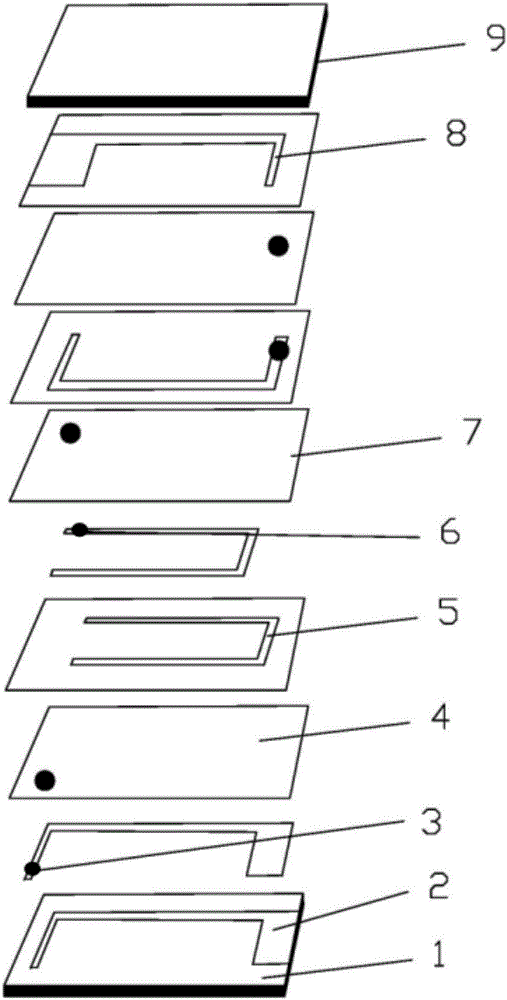
[0040] Embodiment 1: A laminated chip magnetic bead, its structure is as follows figure 1 As shown, the lower substrate 1 and the upper substrate 9 are produced by a dry casting process, the intermediate dielectric films 4 and 7 are produced by a wet casting process, the lower lead-out 2, the upper lead-out 8, the coil 5, the printing point 3 and the 6 are all printed alternately by two screen printing machines. The preparation method comprises the steps of:

[0041] (1) Preparation of slurry:

[0042] Evenly mix the ferrite powder with uniform magnetic permeability and organic solvent, add dispersant, plasticizer and defoamer at the same time, mix the slurry evenly through high-energy ball milling; then add binder and perform secondary ball milling, The mass percentage of each substance is: 56% of ferrite magnetic powder, 5% of PVB adhesive, 35% of organic solvent, 1% of dispersant, 2% of plasticizer, and 1% of defoamer;

[0043] (2) Dry casting:

[0044] Use a high-preci...

Embodiment 2

[0065] Embodiment 2: A laminated chip magnetic bead, its structure is as follows figure 1 As shown, the lower substrate 1 and the upper substrate 9 are produced by a dry casting process, the intermediate dielectric films 4 and 7 are produced by a wet casting process, the lower lead-out 2, the upper lead-out 8, the coil 5, the printing point 3 and the 6 are all printed alternately by two screen printing machines. The preparation method comprises the steps of:

[0066] (1) Preparation of slurry:

[0067] Evenly mix the ferrite powder with uniform magnetic permeability and organic solvent, add dispersant, plasticizer and defoamer at the same time, mix the slurry evenly through high-energy ball milling; then add binder and perform secondary ball milling, The mass percentage of each substance is: ferrite magnetic powder 44%, PVB adhesive 8%, organic solvent 45%, dispersant 1%, plasticizer 1%, defoamer 1%;

[0068] (2) Dry casting:

[0069] A high-precision steel belt casting ma...


PUM

PropertyMeasurementUnit
thicknessaaaaaaaaaa
thicknessaaaaaaaaaa
thicknessaaaaaaaaaa

Abstract

The invention relates to the field of electronic components, in particular to a preparation method of a laminated magnetic bead. A dry casting process is adopted for producing an upper substrate and a lower substrate of the laminated magnetic bead; a wet casting process is adopted for producing an internal dielectric film, and an internal coil of the laminated magnetic bead is manufactured by combining a screen printing process; and an isostatic pressing method is adopted by subsequent procedures, thereby ensuring the consistency of magnet shrinkage rates of a dry method and a wet method. The problems of a long production cycle and low efficiency are solved; and meanwhile, the quality problem of a laminated magnetic bead stress jumper is also solved. According to the preparation method, the magnet shrinkage rate of the magnetic bead is reduced, the production efficiency is improved and the production cycle of the magnetic bead is shortened to within 12 days from 15 days.

Description

technical field [0001] The invention relates to the field of electronic components, in particular to a method for preparing laminated chip magnetic beads. Background technique [0002] The magnetic bead is an inductor filled with a magnetic core. It uses its impedance to increase rapidly at high frequencies and the electromagnetic loss mechanism of magnetic materials to suppress and absorb high-frequency noise, thereby achieving the purpose of anti-electromagnetic interference. Multilayer chip magnetic bead is a high-tech product developed in recent years. With the development of industrial automation, especially the development of modern communication industry (such as mobile phone and other portable terminal products), the multilayer chip magnetic bead is characterized by its Good magnetic shielding, miniaturization and other advantages have become key products in the field of electronic components. Its applications range from mobile devices, computers, servers, personal ...

Claims


Application Information

Patent Timeline
Patent Type & Authority Applications(China)
IPC IPC(8): H01F41/28H01F41/04
CPCH01F41/0233H01F41/042H01F41/28
Inventor 李孔俊高泮嵩
Owner GUANGDONG FENGHUA BANGKE ELECTRONIC CO LTD
Why Eureka
Try Eureka