Wafer-level method for packaging camera modules and related camera modules
A camera module and wafer-level technology, applied in radiation control devices, color TV components, TV system components, etc., can solve the problem of expensive packaging array cameras
- Summary
- Abstract
- Description
- Claims
- Application Information
AI Technical Summary
Problems solved by technology
Method used
Image

Examples
Embodiment Construction
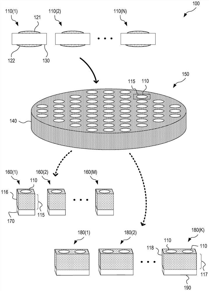
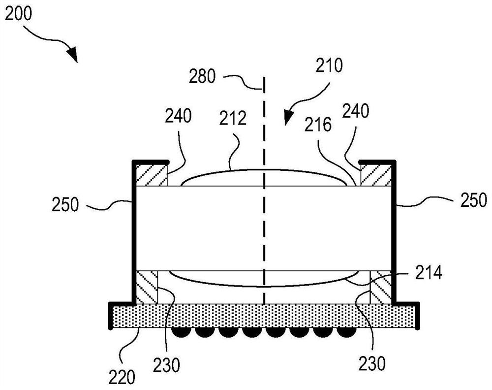
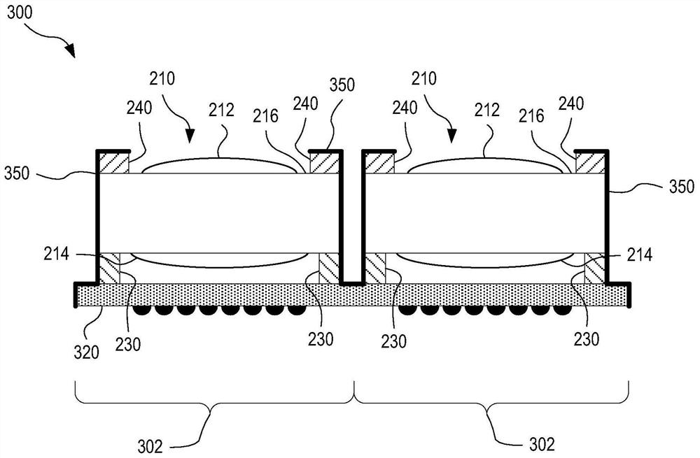
[0029] Disclosed herein are methods for packaging lenses, lens assemblies, and / or camera modules. These approaches are based at least in part on the wafer level and thus can significantly reduce packaging costs compared to non-wafer level approaches. Figure 1-9 The invention relates to a method of packaging a wafer-level lens under the wafer level, so as to construct a lens assembly with an integral housing. The housing may be light-tight except for the viewing area. These lens components are generally bonded to respective image sensors to form a camera module. Figure 10-20BThe invention relates to a method of packaging lens units with respective image sensors at the wafer level, thereby producing housings for use in produced camera modules. These methods eliminate the need for the step of bonding the lens unit to the image sensor, thereby further reducing packaging costs.
[0030] figure 1 An exemplary method 100 for packaging a plurality of wafer-level lenses 110 is sh...
PUM
 Abstract
Description
Claims
Application Information
 - R&D
- Intellectual Property
- Life Sciences
- Materials
- Tech Scout
- Unparalleled Data Quality
- Higher Quality Content
- 60% Fewer Hallucinations
Browse by: Latest US Patents, China's latest patents, Technical Efficacy Thesaurus, Application Domain, Technology Topic, Popular Technical Reports.
© 2025 PatSnap. All rights reserved.Legal|Privacy policy|Modern Slavery Act Transparency Statement|Sitemap|About US| Contact US: help@patsnap.com