
Eureka
For R&D, Eureka makes reading and utilizing patents & technical documents easy.
Eureka AIR
Designed for self-driven R&D workflows. Generate viable solutions, solve complex R&D challenges, empower your innovation with AI.

Eureka Materials
Designed for material experts only. Revolutionize your material R&D, from search, analyze, to developing new materials.

TechResearch
Generate reliable direction feasibility study reports for your R&D in just a few steps.

TechSeek
Discover and master advanced knowledge NOW. Basics, ideas, possibilities, all at once.

TechMind
As an expert in R&D Theories, TechMind can generates customized viable solutions instantly.

TechRisk
Analyze your overall solution with one click, know your potential R&D risks in advance.

TechMonitor
Get weekly tech updates, stay abreast of the latest tech innovations and key insights.
Printed circuit board and liquid crystal display
A printed circuit board and width technology, which is applied in the direction of printed circuit, printed circuit, printed circuit parts, etc., can solve the problems of waste, height increase and pitch increase of anisotropic conductive film, and achieve the increase of design cost and difficulty, The effect of reducing the inflection ratio
- Summary
- Abstract
- Description
- Claims
- Application Information
AI Technical Summary
Problems solved by technology
Method used
Image

Examples
Embodiment 1
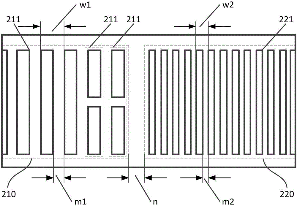
[0029] figure 2 It is a schematic diagram of the local structure of the connection area and the non-connection area of the printed circuit board in the embodiment of the present invention. Combine below figure 2 The specific structure of the printed circuit board will be described in detail.
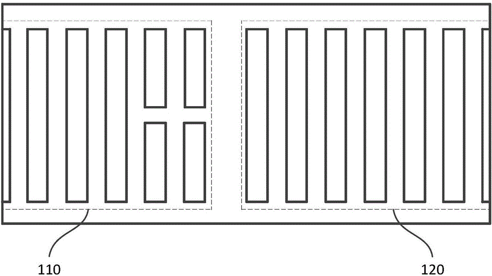
[0030] The printed circuit board is provided with at least one pair of connection area 210 and non-connection area 220 adjacent to each other.
[0031] In a pair of adjacent connection regions 210 and non-connection regions 220, the connection region 210 is equidistantly arranged with a plurality of first gold fingers 211 according to the first pitch m1, and the non-connection region 220 is provided with equidistant intervals according to the second pitch m2. A plurality of second gold fingers 221 . Wherein, the sum of the width of the first golden finger 211 and the first distance m1 is the first unit width w1, and the first unit width w1 satisfies the first width range. The sum...
Embodiment 2
[0038] This embodiment further optimizes the width w1 of the first unit and the width w2 of the second unit in the first embodiment.
[0039] In the first embodiment, the width w1 of the first unit satisfies the first width range, and the width w2 of the second unit satisfies the second width range. On this basis, this embodiment further defines the first width range and the second width range. Specifically, the lower limit of the first width range is preferably set to 400 μm, and the upper limit of the second width range is preferably set to 330 μm.
[0040] It should be noted that the present embodiment does not specifically limit the upper limit of the first width range and the lower limit of the second width range. In the specific implementation process, as long as its size meets the design requirements.
[0041] To sum up, when the width of the first unit becomes larger (greater than 400 μm) according to the requirements of the transmission signal, and the distribution ...
Embodiment 3
[0043] In this embodiment, the width w2 of the second unit in the second embodiment is further optimized.
[0044] In the second embodiment, the width w1 of the first unit satisfies the first width range, the width w2 of the second unit satisfies the second width range, and the lower limit of the first width range is 400 μm, and the upper limit of the second width range is 330 μm. On this basis, in this embodiment, the width w2 of the second unit is more specifically defined, and the width w2 of the second unit is set as a fixed size. Preferably, the width of the second cell is set to 300 μm.
[0045] In order to further demonstrate the technical effect achieved by applying the printed circuit board of this embodiment, the following two cases where the width w1 of the first unit is 440 μm and 500 μm are taken as examples, and the width of the second unit is designed to be 300 μm. Ratio effects were tested.
[0046] There are two types of test machines:
[0047] The first ty...
PUM
| Property | Measurement | Unit |
|---|---|---|
| width | aaaaa | aaaaa |
| width | aaaaa | aaaaa |
Abstract
Description
Claims
Application Information
 - R&D Engineer
- R&D Manager
- IP Professional
- Industry Leading Data Capabilities
- Powerful AI technology
- Patent DNA Extraction
Browse by: Latest US Patents, China's latest patents, Technical Efficacy Thesaurus, Application Domain, Technology Topic, Popular Technical Reports.
© 2024 PatSnap. All rights reserved.Legal|Privacy policy|Modern Slavery Act Transparency Statement|Sitemap|About US| Contact US: help@patsnap.com