Check patentability & draft patents in minutes with Patsnap Eureka AI!

Transistor devices and methods

A technology of transistors and devices, applied in the field of semiconductor devices

Active Publication Date: 2017-05-17
QUALCOMM INC
View PDF4 Cites 0 Cited by
  • Summary
  • Abstract
  • Description
  • Claims
  • Application Information

AI Technical Summary

Problems solved by technology

Existing solutions for reducing these parasitics and for managing high currents and voltages are not optimal for meeting the increasing demands of the electronics industry

Method used


Image

  • Transistor devices and methods
  • Transistor devices and methods
  • Transistor devices and methods

Examples


Embodiment Construction

[0014] The present disclosure pertains to transistor devices and methods. In the following description, for the purposes of explanation, several examples and specific details are set forth in order to provide a thorough understanding of the present disclosure. However, it will be apparent to those skilled in the art that the present disclosure as set forth in the claims may include some and all of the features in these examples alone or in combination with other features described below, and may further include those described herein Modifications and equivalents of features and concepts.

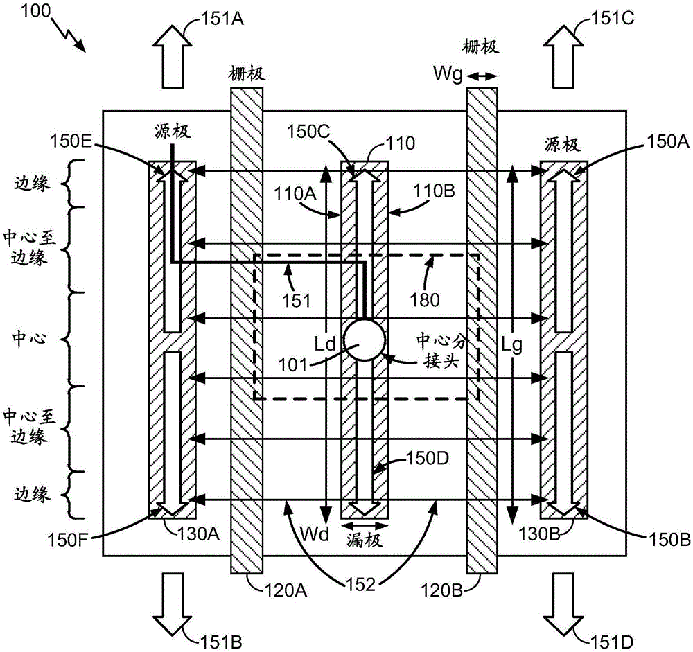
[0015] figure 1 An exemplary transistor 100 is shown according to one embodiment. In this example, transistor 100 is a metal oxide semiconductor field effect transistor (MOSFET). Transistor 100 includes drain 110, gates 120A-B, and sources 130A-B. In this example, the source and gate include two structures 120A and 120B on opposite sides 110A and 110B of drain 110 . Specifically, the ...


PUM


Abstract

The present disclosure includes transistor devices and methods. In one embodiment, a transistor includes a gate, a source, and a drain. According to one aspect of the disclosure, different resistive paths in the drain are compensated using different gate-to-drain capacitances. According to another aspect of the disclosure, current enters a drain at a center tap point and flows symmetrically outward under two adjacent gates to two adjacent sources.

Description

[0001] CROSS-REFERENCE TO RELATED APPLICATIONS [0002] This application claims priority to US Application No. 14 / 486,969, filed September 15, 2014, the contents of which are hereby incorporated by reference in their entirety for all purposes. technical field [0003] The present disclosure relates to semiconductor devices and methods, and in particular to transistor devices and methods. Background technique [0004] The performance requirements placed on electronic circuits continue to gradually increase. The basic building block of almost all electronic circuits is the transistor. As transistors operate at even higher and higher speeds, parasitic effects within the device are increasingly becoming a problem. For example, when current flows through the terminals of a transistor device, the internal resistance can cause a voltage drop, which can drain the circuit's power and reduce the circuit's efficiency. This internal resistance can impose limitations on the size of t...

Claims


Application Information

Patent Timeline
Patent Type & Authority Applications(China)
IPC IPC(8): H01L29/40H01L29/417H01L29/78H03K17/16H01L23/522
CPCH01L29/402H01L29/41758H01L29/41775H01L29/7824H01L29/7835H03K17/162H01L23/522H01L2924/0002H01L2924/00H01L29/78624H01L29/7816
Inventor A·斯库德里
Owner QUALCOMM INC
Features
  • R&D
  • Intellectual Property
  • Life Sciences
  • Materials
  • Tech Scout
  • Unparalleled Data Quality
  • Higher Quality Content
  • 60% Fewer Hallucinations
Learn More