Chip automatic tinning device

A chip and automatic technology, applied in the field of chip manufacturing, can solve the problems of easy short circuit of pins, low efficiency of tinning, easy to pollute chips, etc., and achieve the effects of not easy short circuit and deformation, high efficiency of tinning, and precise control of tinning height

Inactive Publication Date: 2017-05-31
BEIJING INST OF COMP TECH & APPL
View PDF3 Cites 5 Cited by
  • Summary
  • Abstract
  • Description
  • Claims
  • Application Information

AI Technical Summary

Problems solved by technology

[0003] The purpose of the present invention is to provide an automatic tinning device for chips, which is used to solve the problems of poor consistency in the tinning operation of the o...

Method used


Image

  • Chip automatic tinning device

Examples


Embodiment Construction

[0013] In order to make the purpose, content, and advantages of the present invention clearer, the specific embodiments of the present invention will be further described in detail below with reference to the accompanying drawings and embodiments.

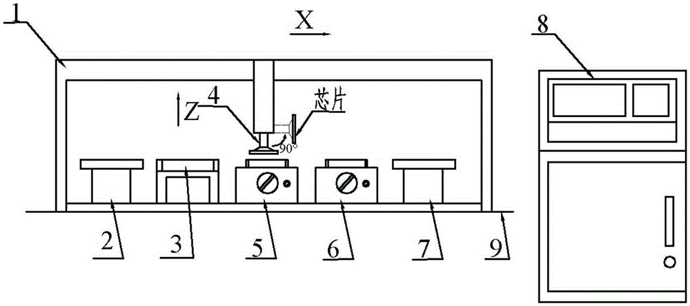
[0014] figure 1 Shown is the schematic diagram of the chip automatic tinning device, such as figure 1 As shown, the chip automatic tinning device includes: a four-axis tinning working platform 1, a chip positioning device 2, a flux tank 3, a vacuum suction cup device 4, a tin pot 5, a tin pot 6, a chip recovery device 7 and a control cabinet 8.

[0015] like figure 1 As shown, the vacuum chuck seat 4, the chip positioning device 2, the flux tank 3, the tin pot 5, the tin pot 6, and the chip recovery device 7 are integrated and installed on the mechanical body of the four-axis tinning working platform 1, and the whole tinning movement process It is controlled by the control cabinet 8 .

[0016] refer to figure 1 , the chip posit...


PUM


Abstract

The invention discloses a chip automatic tinning device. The chip automatic tinning device comprises a four-shaft tinning working platform, a chip positioning device, a flux tank, at least one tin pot and a control device; the chip positioning tool is used for positioning a chip on the chip positioning tool to determine the center position of the chip; the control device is used for controlling actions of the four-shaft tinning working platform according to the center position of the chip; the at least one tin pot is used for tinning the chip; and the flux tank is used for adding a flux to the chip. The chip automatic tinning device can precisely control the tinning height to achieve good consistency, is not liable to generate short circuit and deformation for pins, has no need to hold the chip by a hand for operation, is not influenced by the physical power of people, is high in tinning efficiency, and can prevent pollution of the chip by the hand and risks possibly caused by static electricity of human bodies.

Description

technical field [0001] The invention relates to the technical field of chip manufacturing, in particular to an automatic tinning device for chips. Background technique [0002] The tinning operation of the existing chip is completed by the operator holding the chip, which has the following problems: the height of the tinning is not easy to control, the flatness is not good, and the precision of the tinning is low; the pins are easily short-circuited and the pins are deformed; the tinning efficiency is low, People who want to hold the chip will not be able to operate it for a long time due to the influence of force; the hands have oil stains, gray marks, etc., which are easy to contaminate the chip and reduce the solderability; there is a risk of damage to the chip due to static electricity on the human body. SUMMARY OF THE INVENTION [0003] The object of the present invention is to provide an automatic tinning device for chips, which is used to solve the problems of poor ...

Claims


Application Information

Patent Timeline
IPC IPC(8): C23C2/08
CPCC23C2/08
Inventor 陈俊桃张志华张永忠
Owner BEIJING INST OF COMP TECH & APPL
Why Eureka
Try Eureka