Touch panel and manufacturing method thereof as well as display device

A touch panel and transistor technology, which is applied to instruments, electrical digital data processing, and input/output processes of data processing, etc., can solve the problems of inability to achieve full-screen fingerprint collection, reduced display light transmittance, and difficulty in fingerprint collection, etc. Achieve the effect of full-screen optical fingerprint acquisition, high-precision full-screen optical fingerprint acquisition, and narrow spacing

Active Publication Date: 2017-05-31
BOE TECH GRP CO LTD
View PDF5 Cites 14 Cited by
  • Summary
  • Abstract
  • Description
  • Claims
  • Application Information

AI Technical Summary

Problems solved by technology

At present, OLED display devices can realize touch sensing by applying capacitive touch technologies such as in-cell, on-cell and out-cell, but it is still difficult Acquisition of fingerprints by capacitive touch
In this regard, although some optical fingerprint sensors and radio frequency fingerprint sensors can realize fingerprint collection in a small area outside the display area, because they will reduce the display light transmittance, it is difficult to set them in the full screen range, so full-screen fingerprint collection cannot be realized

Method used


Image

  • Touch panel and manufacturing method thereof as well as display device
  • Touch panel and manufacturing method thereof as well as display device
  • Touch panel and manufacturing method thereof as well as display device

Examples


Embodiment Construction

[0052] In order to make the object, technical solution and advantages of the present invention clearer, the implementation manner of the present invention will be further described in detail below in conjunction with the accompanying drawings.

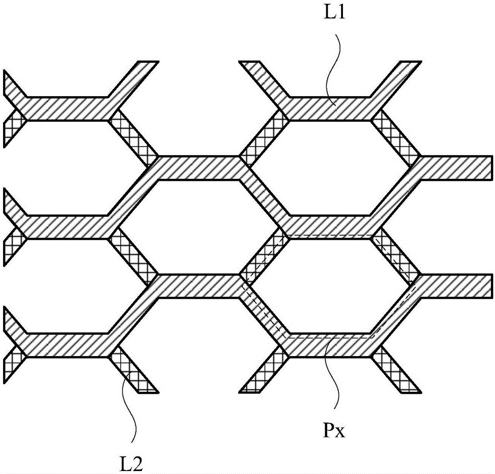
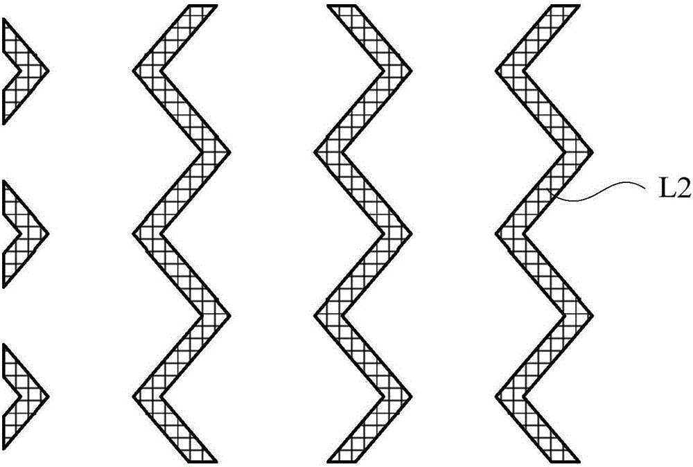
[0053] figure 1 It is a schematic diagram of an arrangement method of sub-pixel regions in a touch panel provided by an embodiment of the present invention. see figure 1 , the touch panel of the embodiment of the present invention has a plurality of first signal lines L1 and a plurality of second signal lines L2, wherein the patterns of the plurality of second signal lines L2 are as follows figure 2 shown. compare figure 1 and figure 2 It can be seen that the intersections of the multiple first signal lines L1 and the multiple second signal lines L2 define several sub-pixel regions Px.

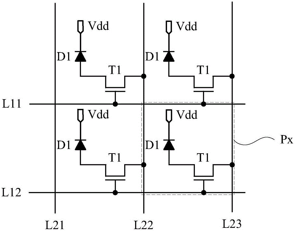
[0054] image 3 It is a schematic diagram of the circuit structure in the touch panel provided by the embodiment of the present invention. se...


PUM


Abstract

The invention discloses a touch panel and a manufacturing method thereof as well as a display device, and belongs to the field of touch control. The control panel comprises a plurality of first signal lines and a plurality of second signal lines that cross one another to define a plurality of sub-pixel areas including a pixel opening area; a transistor and a photosensitive element are disposed in each sub-pixel area, wherein the gate of the transistor is connected to one of the plurality of first signal lines, and one of the source and the drain is connected to one of the plurality of second data lines, while the other one is connected to the first pole of the photosensitive element in the respective sub-pixel area, wherein the photosensitive element is disposed in a sub-pixel area except for the disposal area of the transistor and the pixel opening area. The touch panel also comprises a transparent electrode layer. The second pole of each photosensitive element is connected to the transparent electrode layer. In addition, each photosensitive element is configured to generate a light intensity sensing signal between the first pole and the second pole thereof based on the detected light intensity. According to the invention, full-screen fingerprint acquisition of a display device may be achieved.

Description

technical field [0001] The present invention relates to the field of touch control, in particular to a touch panel, a manufacturing method thereof, and a display device. Background technique [0002] Electroluminescence device is a kind of self-luminous display device, which has attracted wide attention due to its advantages such as wide viewing angle, high contrast ratio and high response speed. With the development of the field of electroluminescence, organic electroluminescent devices (such as organic light emitting diodes, Organic Light Emitting Diode, OLED) can achieve more excellent brightness, driving voltage, response rate and Therefore, it has become the mainstream of the current display market. At present, OLED display devices can realize touch sensing by applying capacitive touch technologies such as in-cell, on-cell and out-cell, but it is still difficult Fingerprint collection is realized by capacitive touch. In this regard, although some optical fingerprint ...

Claims


Application Information

Patent Timeline
Patent Type & Authority Applications(China)
IPC IPC(8): G06F3/041G06F3/044
CPCG06F3/0412G06F3/044G06F2203/04103
Inventor 许睿董学王海生刘英明王晨如孙剑唐贞郭玉珍刘伟
Owner BOE TECH GRP CO LTD
Why Eureka
Try Eureka