Photoelectric detector based on PtSe2 and silicon nanorod array and preparation method of photoelectric detector

A photodetector, silicon nanopillar technology, applied in nanotechnology, nanotechnology, nanotechnology and other directions for sensing, can solve the problem of low photoresponsivity of photodetector, small effective area of ​​heterojunction, and degradation of device performance and other problems, to achieve the effect of improving the photoelectric conversion efficiency, increasing the effective contact area, and improving the integral sensitivity

Active Publication Date: 2021-06-01
XIAN TECH UNIV
View PDF11 Cites 2 Cited by
  • Summary
  • Abstract
  • Description
  • Claims
  • Application Information

AI Technical Summary

Problems solved by technology

[0003] However, most photodetectors based on two-dimensional materials are still limited in practical applications, because the thickness of single-layer or few-layer two-dimensional materials is only a few nanometers, the absorption rate of incident light is less than 10%, and Planar semiconductors such as silicon have strong light reflection, which leads to a relatively low responsivity of photodetectors formed by two-dimensional materials and planar silicon and other semiconductor planes
However, whether it is a nanowire array or a nanocone array, their contact with graphene mainly depends on the tip contact, so that the effective area of ​​the heterojunction is small, which will bring a large contact resistance to the device, which also restricts the device. Photoelectric conversion efficiency
Secondly, most of the current two-dimensional material layers of photodetectors have to undergo multiple transfers when they are combined with other traditional semiconductors such as silicon, germanium, gallium arsenide, etc., and transfer carriers such as PMMA need to be removed. Similar photodetection devices need to prepare metal electrodes on the two-dimensional material layer and other semiconductor surfaces, that is, at least two steps are required to complete the electrode preparation, and these processes will inevitably cause a certain degree of damage and pollution to graphene. , leading to defects in the interface between the final two-dimensional material and the semiconductor, which will lead to a decrease in the performance of the final device
[0004] To sum up, the preparation process of mainstream photodetectors based on two-dimensional materials requires more material transfer times, and the electrode needs at least two steps to complete the preparation, which not only increases the cost, but also makes the contact surface between graphene and semiconductor more difficult. The cleanliness decreases and the defects increase, making it difficult to form a high-quality PN junction
Photodetectors composed of vertically stacked semiconductors and two-dimensional materials have low photoresponsivity, and the photoelectric conversion efficiency is greatly limited.
Although detectors equipped with nanowire arrays or nanocone array light-trapping structures have higher light absorption rate, the smaller heterojunction contact area will still reduce the photoelectric conversion efficiency of the device.

Method used


Image

  • Photoelectric detector based on PtSe2 and silicon nanorod array and preparation method of photoelectric detector
  • Photoelectric detector based on PtSe2 and silicon nanorod array and preparation method of photoelectric detector
  • Photoelectric detector based on PtSe2 and silicon nanorod array and preparation method of photoelectric detector

Examples


Embodiment 1

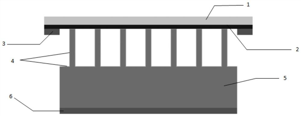
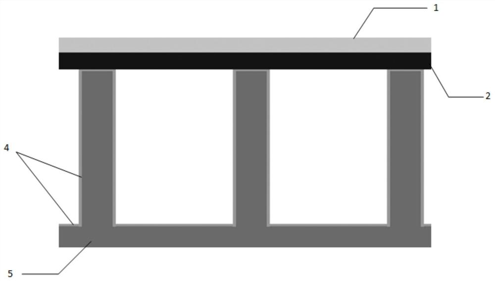
[0058] 1. Soak the cut copper foil (thickness 25 μm, purity 99.99%) in acetone for 5 minutes, then put it in an ultrasonic machine for 10 seconds, pour off the acetone and use ethanol to ultrasonically clean it for 5 minutes, and finally rinse it several times with deionized water. And blow off the surface moisture with a nitrogen gun. The treated copper foil is placed on the quartz slide and pushed to the position near the thermocouple in the heating zone in the middle of the outer end of the quartz tube. After evacuating to about 4Pa, argon is introduced to normal pressure, and the above process is repeated to reduce the oxygen content and prevent the copper foil from being oxidized under high temperature conditions. Keep the first path of Ar gas (Ar1, 500mL / min), H 2 (30mL / min) The flow rate remains unchanged, the program control is started for 90min, and the temperature is raised to 1000°C at a constant speed. Subsequent heat preservation and preheating treatment for 2 h...

Embodiment 2

[0065] 1. Cut the copper foil (thickness 25μm, purity 99.99%) into the required size, then ultrasonically clean it with acetone and alcohol for 15 minutes, then treat it with 20% dilute hydrochloric acid for 20 minutes, and finally add acetone, alcohol and Ultrasonic cleaning in deionized water for 10 min and blowing off the surface moisture with a nitrogen gun. The cleaned and dried copper foil is placed in the constant temperature zone of the tube furnace, and the sealed quartz tube is fed with Ar gas with a flow rate of 1100 sccm and hydrogen gas with a flow rate of 20 sccm, and the tube furnace is heated to 1000 °C at a heating rate of 10 °C / min. Subsequently, the hydrogen flow rate was adjusted to 100 sccm for heat preservation and preheating treatment for 60 minutes, so that the arrangement of copper atoms tended to be consistent, and at the same time, the surface activity of copper foil was improved, thereby promoting the deposition of carbon atoms. After the heat prese...


PUM

PropertyMeasurementUnit
diameteraaaaaaaaaa
thicknessaaaaaaaaaa
thicknessaaaaaaaaaa

Abstract

The invention discloses a photoelectric detector based on PtSe2 and a silicon nanorod array and a preparation method of the photoelectric detector. The photoelectric detector comprises a PMMA light-transmitting protective layer, a transparent upper graphene electrode, a silicon nanopillar array structural body coated with few layers of PtSe2, and a metal electrode of the transparent upper graphene electrode and the silicon nanopillar array structural body. The preparation method comprises the following steps: preparing graphene by a CVD method; preparing a silicon nanopillar array structural body by dry etching; coating the surface of the silicon nanopillar array structure body with a few layers of PtSe2 by laser interference enhanced induction CVD; preparing the transparent upper graphene electrode; and plating the metal electrode through magnetron sputtering. The photoelectric detector prepared by the invention can realize detection in a range of visible light to near-infrared bands; and the silicon nanopillar array structure enhances the light absorption effect of the detector, so the detector has the advantages of high sensitivity, simple device structure and high practicability. Meanwhile, the preparation method can improve the performance of the detector, and has a relatively high popularization value.

Description

technical field [0001] The invention relates to the field of optoelectronic technology, in particular to the field of photodetectors. More specifically, a PtSe-based 2 Photodetectors with arrays of silicon nanopillars and methods for their fabrication. Background technique [0002] Photodetectors convert light radiation energy into electricity through physical effects such as photon effect or photothermal effect to realize the detection of light radiation. Photodetectors are widely used in various fields of military and national economy. In the visible or near-infrared band, it is mainly used for ray measurement and detection, industrial automatic control, photometry, etc.; in the infrared band, it is mainly used for missile guidance, infrared thermal imaging, infrared remote sensing, etc. Before the discovery of graphene, traditional semiconductors (such as Si, GaN, InGaAs, InSb, HgCdTe, etc.) have always occupied a dominant position in the photodetector market. From th...

Claims


Application Information

Patent Timeline
Patent Type & Authority Applications(China)
IPC IPC(8): H01L31/109H01L31/18H01L27/144B82Y40/00B82Y15/00
CPCH01L31/109H01L31/18H01L27/1443H01L27/1446B82Y15/00B82Y40/00C23C16/045C23C16/047C23C16/305C23C16/4481C23C16/483H01L31/035227H01L31/032H01L31/036Y02P70/50C23C14/35H01L31/022466H01L31/1864H01L31/1888
Inventor 刘欢杜宇轩贾金梅赵季杰文帅白民宇解飞谢万鹏杨媚吴嘉元刘卫国
Owner XIAN TECH UNIV
Why Eureka
Try Eureka