Image sensor and manufacturing method thereof

A technology of image sensor and manufacturing method, which is applied in the direction of radiation control devices, etc., can solve the problems of reducing the ability of anti-radiation, small effective photosensitive area, and affecting normal work, so as to maintain anti-irradiation, eliminate valve effect, and good anti-irradiation The effect of soft failure

Inactive Publication Date: 2011-12-28
SHANGHAI ADVANCED RES INST CHINESE ACADEMY OF SCI
View PDF8 Cites 2 Cited by
  • Summary
  • Abstract
  • Description
  • Claims
  • Application Information

AI Technical Summary

Problems solved by technology

[0010] like image 3 The first structure shown can guarantee the anti-radiation effect, but because the top layer silicon 204a is too thin, the commonly used vertical photodiode structure cannot be made deep enough, resulting in a very low absorption rate of red light with a longer wavelength, and effective photosensitive small area; Figure 4 Although the second structure shown can make the photosensitive diode 207b deep enough on the bulk silicon (silicon substrate) 201b to ensure the absorptivity of red light, but because of the loss of the protection of the buried oxide layer above, resulting in Electron holes enter the photodiode, increasing the dark current, greatly reducing its ability to resist radiation, and affecting its normal work

Method used


Image

  • Image sensor and manufacturing method thereof
  • Image sensor and manufacturing method thereof
  • Image sensor and manufacturing method thereof

Examples


Embodiment Construction

[0051] The present invention will be further described below in conjunction with specific embodiment and accompanying drawing, set forth more details in the following description so as to fully understand the present invention, but the present invention can obviously be implemented in a variety of other ways different from this description, Those skilled in the art can make similar promotions and deductions based on actual application situations without violating the connotation of the present invention, so the content of this specific embodiment should not limit the protection scope of the present invention.

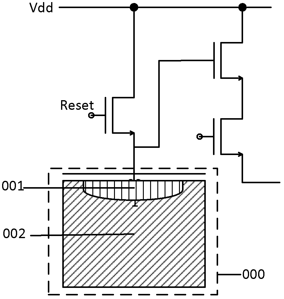
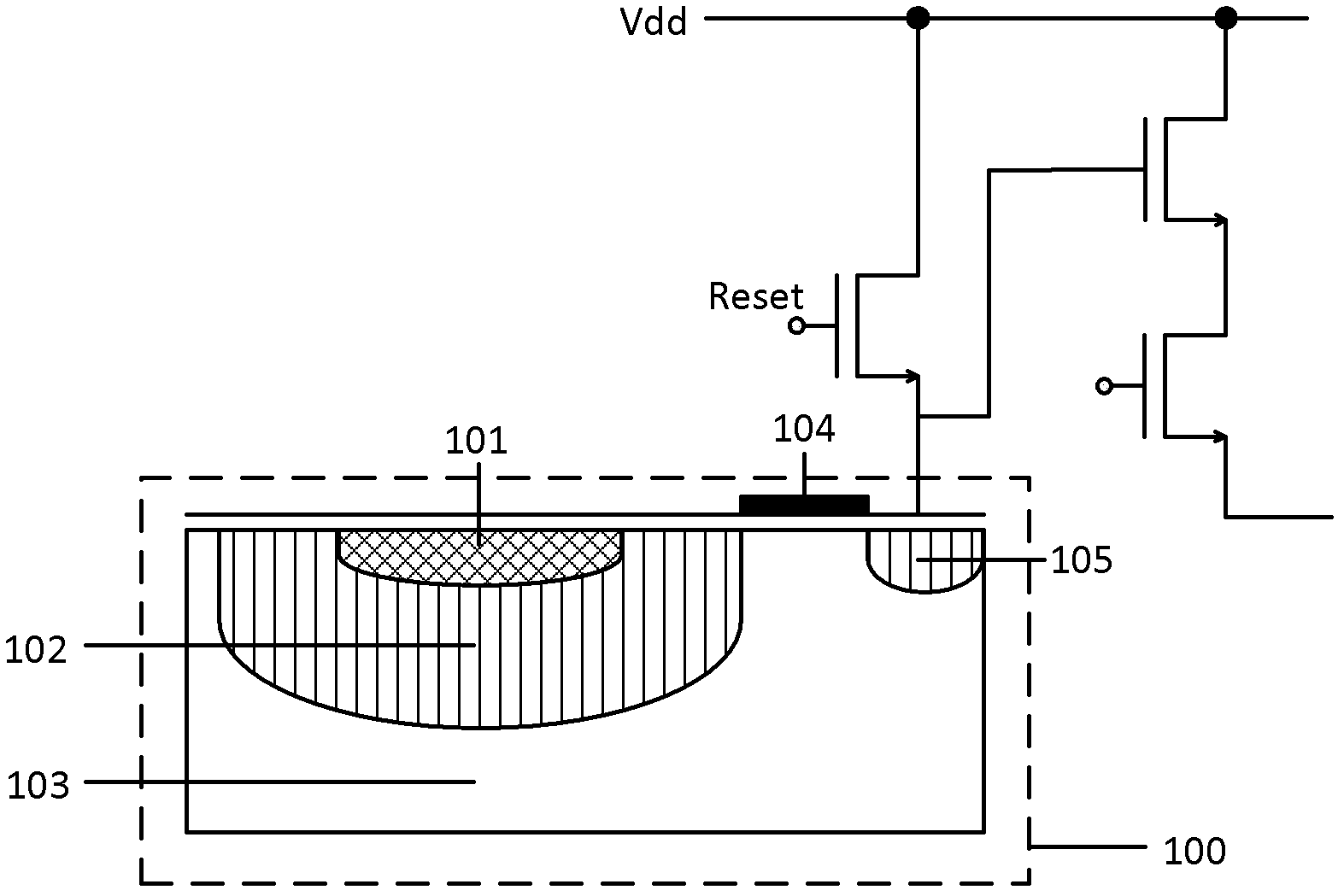
[0052] In the manufacturing process of the image sensor of one embodiment of the present invention, include:

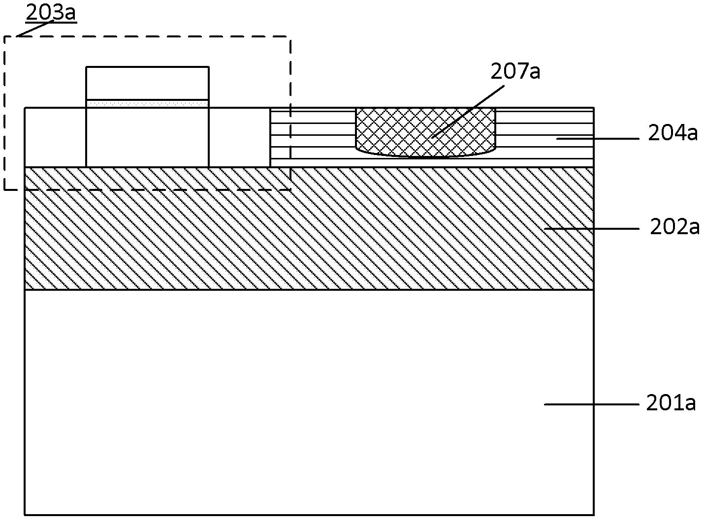
[0053] Executing the first step to provide a semiconductor substrate, which sequentially includes a top semiconductor layer, an insulating layer and a supporting substrate from top to bottom;

[0054] performing a second step of fabricating both the photodiode ...


PUM


Abstract

The invention provides a method for manufacturing an image sensor, comprising the steps of: providing a semiconductor substrate, which sequentially includes a top semiconductor layer, an insulating layer, and a supporting substrate from top to bottom; fabricating a photosensitive diode and a signal readout circuit on the top semiconductor substrate; on the layer; connecting the two through metal interconnection; wherein, the fabrication of the photodiode includes the steps of: selecting the fabrication region; forming the first and second doped regions respectively, the second doped region surrounds the first doped region, and There is a fully depleted region between them; the fully depleted region is doped; and the semiconductor substrate is annealed at high temperature. Correspondingly, the present invention also provides an image sensor. The present invention adopts a lateral photosensitive diode, and manufactures a three-layer surrounding structure of the first conductivity type doped region / full depletion region / second conductivity type doped region on the top semiconductor layer of the semiconductor substrate, which overcomes the conventional semiconductor Under the process, the photogenerated current is too small and the sensor sensitivity is too low.

Description

technical field [0001] The invention relates to the technical field of semiconductor devices and processes, in particular, the invention relates to an image sensor and a manufacturing method thereof. Background technique [0002] CMOS image sensor is composed of photosensitive pixels and CMOS signal readout circuit. Compared with traditional CCD image sensors, CMOS image sensors have better integration because they adopt CMOS standard manufacturing process, and can be integrated with other digital-analog operations and control circuits on the same chip, which is more suitable for future development trends. [0003] According to the number of transistors contained in photosensitive pixels, CMOS image sensors are mainly divided into 3T (including 3 NMOS transistors) types (such as figure 1 shown) and 4T (with 4 NMOS transistors) type (such as figure 2 shown) two. [0004] Among the photosensitive pixels of CMOS image sensors, the most commonly used photodiode structures in...

Claims


Application Information

Patent Timeline
IPC IPC(8): H01L27/146
Inventor 田犁郭洪量汪辉陈杰汪宁尚岩峰
Owner SHANGHAI ADVANCED RES INST CHINESE ACADEMY OF SCI
Why Eureka
Try Eureka