Infrared detector and manufacturing method thereof

A technology of infrared detectors and manufacturing methods, which is applied in the direction of electric radiation detectors, manufacturing microstructure devices, semiconductor/solid-state device components, etc., can solve the problems of product fill factor decline, sensitive resistance uniformity decline, and small signal. Achieve the effect of increasing photosensitive area and filling factor, improving sensitivity and uniformity, and improving uniformity and consistency

Pending Publication Date: 2020-11-03
SHANGHAI INTEGRATED CIRCUIT RES & DEV CENT
View PDF0 Cites 2 Cited by
  • Summary
  • Abstract
  • Description
  • Claims
  • Application Information

AI Technical Summary

Problems solved by technology

[0008] In order to improve the uniformity in the detector plane and in the chip, the designer will define the graphic size of the above-mentioned micro-bridge plane as large enough as possible (that is, the conductor length L in the above formula is relatively long), which causes the resistance value of the sensitive resistor to be large enough. relatively bigger
At the same time, since the sensitive layer itself is a high-resistance material with high resistivity, it further leads to a large sensitive resistance and a small signal at the same voltage
[0009] Moreover, when forming the micro-bridge plane, the various patterning (lithography / etching) processes adopted for each film layer on the micro-bridge plane also lead to a decrease in the uniformity of the sensitive resistance
[0010] In addition, traditional technology uses multiple support and electrical connection posts, which leads to a decrease in product fill factor

Method used


Image

  • Infrared detector and manufacturing method thereof
  • Infrared detector and manufacturing method thereof
  • Infrared detector and manufacturing method thereof

Examples


Embodiment Construction

[0037] The specific embodiment of the present invention will be further described in detail below in conjunction with the accompanying drawings.

[0038] It should be noted that in the following specific embodiments, when describing the embodiments of the present invention in detail, in order to clearly show the structure of the present invention for the convenience of description, the structures in the drawings are not drawn according to the general scale, and are drawn Partial magnification, deformation and simplification are included, therefore, it should be avoided to be interpreted as a limitation of the present invention.

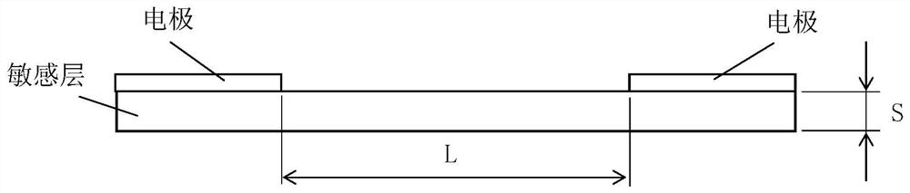
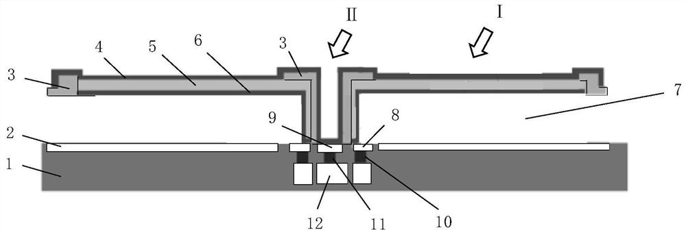
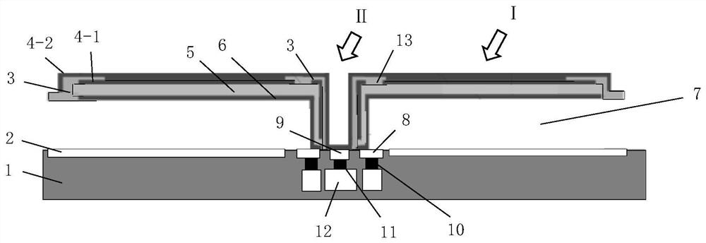
[0039] In the following specific embodiments of the present invention, please refer to figure 2 , figure 2It is a structural schematic diagram of an infrared detector in a preferred embodiment 1 of the present invention. Such as figure 2 As shown, an infrared detector of the present invention includes: a substrate 1 and an infrared microbridge d...


PUM


Abstract

The invention discloses an infrared detector, and the infrared detector comprises a substrate and an infrared micro-bridge deck; the micro-bridge deck is suspended on the substrate through a support and an electric connecting column, and the support and the electric connecting column are arranged below the micro-bridge deck, so the micro-bridge deck forms a suspended structure taking the support and the electric connecting column as centers; the micro-bridge deck comprises a lower electrode layer, a sensitive layer and an upper electrode layer which are sequentially connected from bottom to top, and the lower electrode layer, the sensitive layer and the upper electrode layer further extend into the supports and the electric connecting columns to form structural components of the micro-bridge deck. The lower electrode layer and the upper electrode layer are isolated from each other, are led out downwards along the support and the electric connecting columns, and are respectively connected with a processing circuit arranged in the substrate. According to the invention, the resistance value of the sensitive resistor can be reduced, the uniformity and consistency of pixels can be improved, and the photosensitive area and the fill factor can be effectively improved, so that the sensitivity and uniformity can be obviously improved. The invention further discloses a manufacturing method of the infrared detector.

Description

technical field [0001] The invention relates to the technical field of semiconductor integrated circuits and sensors, in particular to an infrared detector with high sensitivity and high uniformity and a manufacturing method thereof. Background technique [0002] Traditional infrared MEMS detector products generally adopt a microbridge resonant cavity structure, and its sensitive resistance is defined on the plane of the surface of the microbridge, that is, its sensitive resistance is defined by the plane electrode pattern on the sensitive layer. [0003] Please refer to figure 1 , figure 1 It is a distribution form of sensitive resistance electrodes of traditional infrared MEMS detectors. Such as figure 1 As shown, in the traditional infrared MEMS detector structure, a sensitive layer is arranged on the surface of the micro-bridge, and a metal electrode is respectively arranged on the left and right ends of the sensitive layer to form a sensitive resistance structure in ...

Claims


Application Information

Patent Timeline
IPC IPC(8): B81B7/02B81C1/00G01J5/20
CPCB81B7/02B81C1/00015G01J5/20B81B2201/02
Inventor 康晓旭唐晨晨邱佳梦
Owner SHANGHAI INTEGRATED CIRCUIT RES & DEV CENT
Why Eureka
Try Eureka