Pixel array with enlarged photosensitive area

A technology of pixel array and photosensitive area, applied in the field of pixel array, can solve the problems of increasing crosstalk CrossTalk, low utilization efficiency of incident light, narrowing of photodiode PD spacing, etc., to achieve the effect of increasing the possibility of crosstalk CrossTalk

Active Publication Date: 2013-08-07
SHANGHAI INTEGRATED CIRCUIT RES & DEV CENT
View PDF6 Cites 2 Cited by
  • Summary
  • Abstract
  • Description
  • Claims
  • Application Information

AI Technical Summary

Problems solved by technology

[0004] see figure 1 and figure 2 As shown, the pixel array used in the charge-coupled image sensor CIS makes the use of the incident light inefficient due to the following possible reasons:
[0005] (1) Under the condition of a given photosensitive area and number of pixels of the sensor, on the one hand, due to the fixed surface area of ​​the photodiode Photo Diode (referred to as PD), on the other hand, the spacing between pixels is fixed, so it is difficult to improve the dynamic range of the sensor
However, for the traditional Bayer mode, on the one hand, it means that the metal layer for transmitting signals must be thinned, which leads to the reduction of usable electronic devices; on the other hand, it means that the distance between photodiodes PD is reduced, which increases crosstalk. Possibility of Cross Talk

Method used


Image

  • Pixel array with enlarged photosensitive area
  • Pixel array with enlarged photosensitive area
  • Pixel array with enlarged photosensitive area

Examples


Embodiment Construction

[0039] The implementation of the present invention will be described in detail below in conjunction with the drawings and examples, so that the realization process of how to use technical means to solve technical problems and achieve technical effects in the present invention can be fully understood and implemented accordingly.

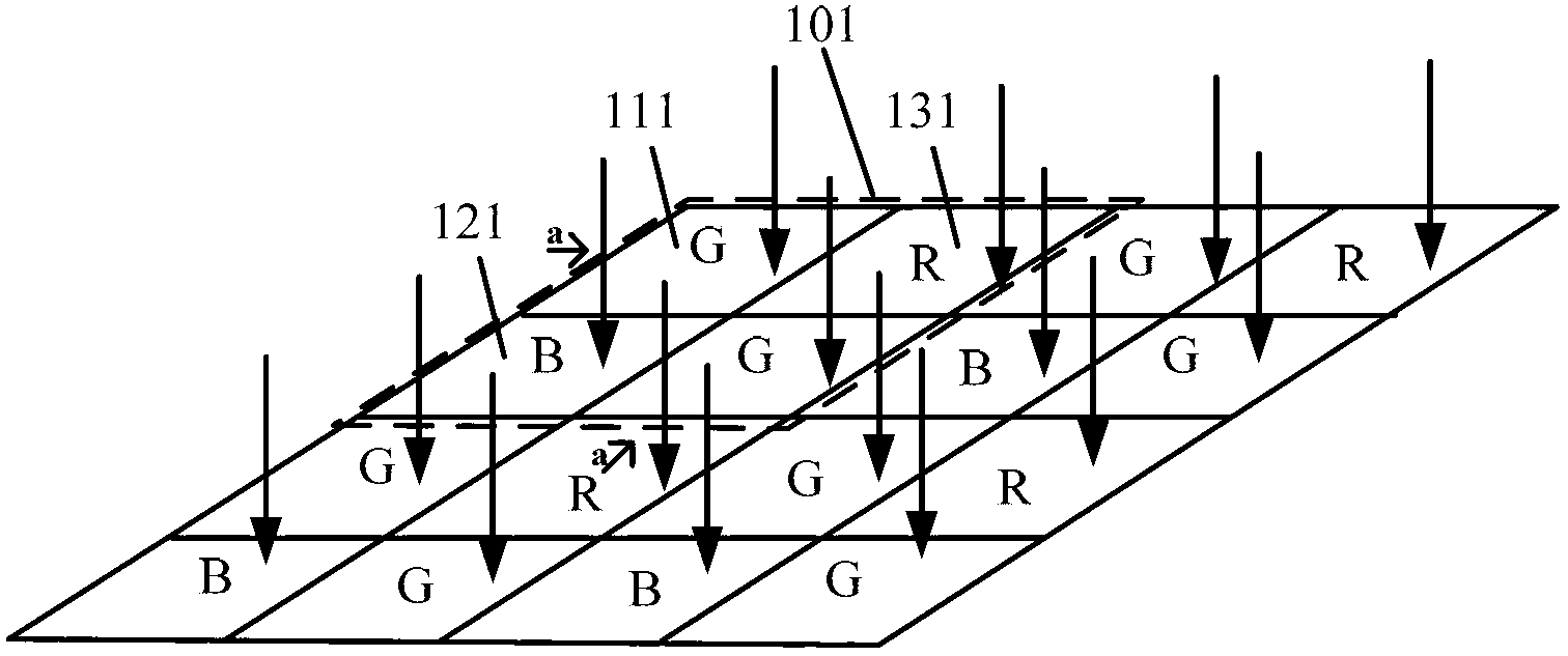
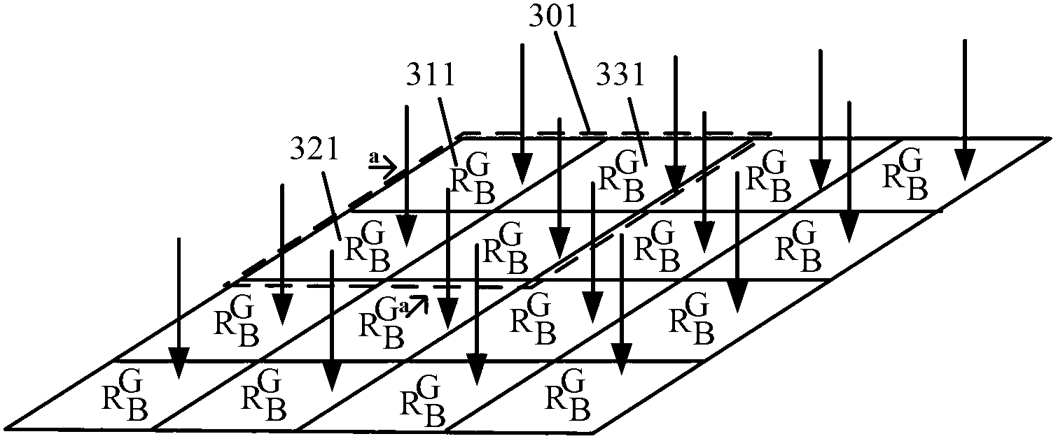
[0040] In the following embodiments of the present invention, the Bayer mode is used as the mode of the pixel array for illustration, but those skilled in the art can understand that, inspired by the following embodiments, the technical solution of the present invention can be applied to other modes The pixel array, the detailed process will not be repeated below.

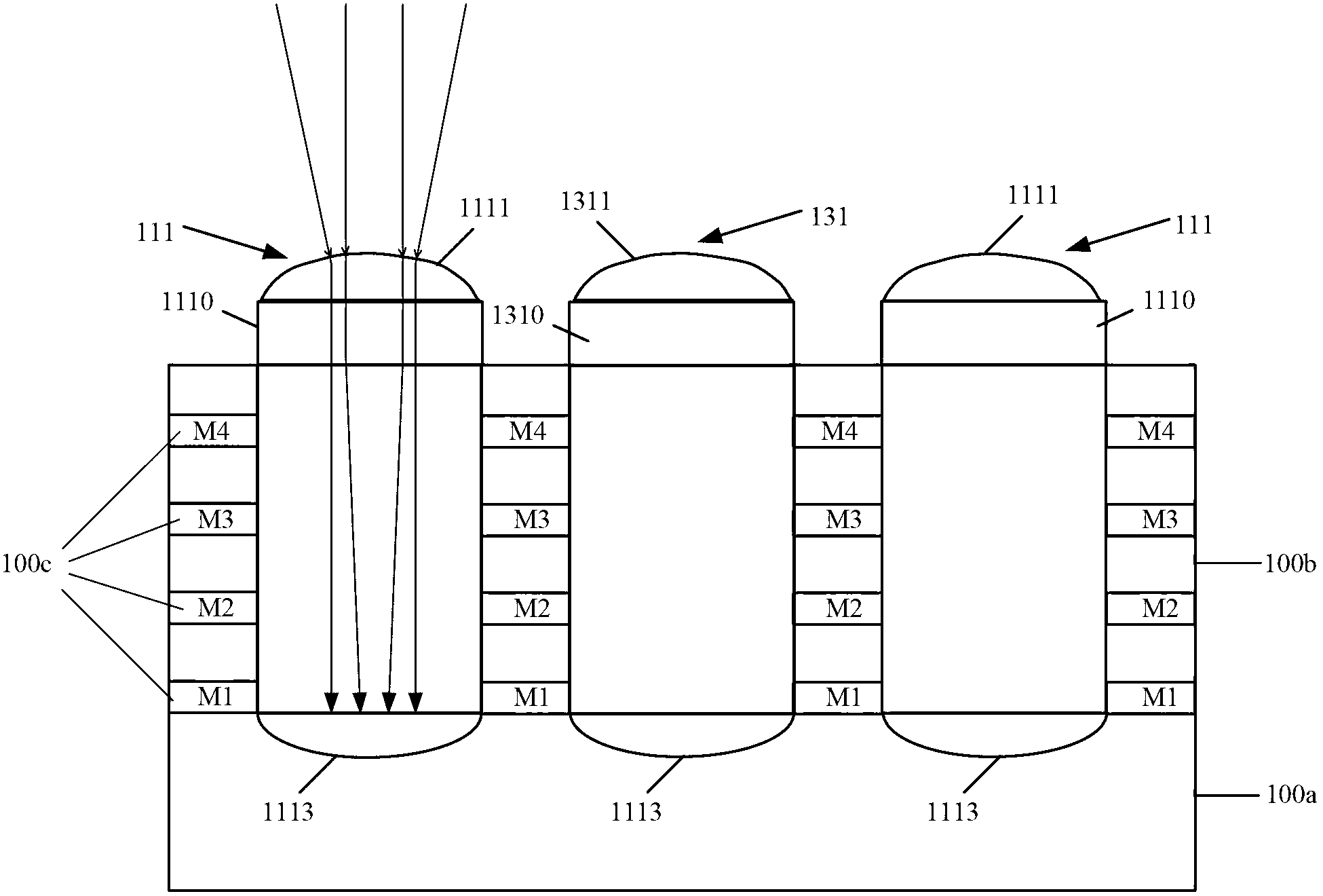
[0041] Since the junction of the photosensitive element can only grow on the silicon material, therefore, in the following embodiments of the present invention, the bottom position of the original optical channel is continuously hollowed out to obtain a cuboid space in the silicon material ...


PUM


Abstract

The invention discloses a pixel array with an enlarged photosensitive area and belongs to the field of integrated circuits. Each unit color restoration module of the pixel array comprises four sub pixels, an optical channel of each sub pixel is divided into a plurality of levels from top to bottom, different photosensitive elements and corresponding spectral elements are selectively arranged along the optical channel of different levels for processing spectrally incident light in the optical channel so as to be sensed by the corresponding photosensitive elements, and the photosensitive elements can be embedded on four random side walls and bottom of the optical channel. Compared with the prior art, photosensitive units are selectively and longitudinally arranged in the optical channel, and meanwhile, a filtering mirror in the prior art is omitted, corresponding spectral units are arranged for the photosensitive units arranged in the optical channel so as to guide or reflect photons matched with the photosensitive units to the photosensitive units, and accordingly electron devices in use are prevented from reducing, and possibility of Cross Talk is prevented from increasing.

Description

technical field [0001] The invention belongs to the field of integrated circuits, and in particular relates to a pixel array with enlarged photosensitive area. Background technique [0002] Image sensors are widely used in civil and commercial applications. Currently, the image sensor consists of a CMOS image sensor (CMOS IMAGE SENSOR, hereinafter referred to as CIS) and a charge-coupled image sensor (Charge‐coupled Device, hereinafter referred to as CCD). For CCDs, on the one hand, in professional scientific research and industrial fields, CCDs with high signal-to-noise ratio are the first choice; on the other hand, in the field of high-end photography, CCDs that can provide high image quality are also popular. For CIS, it is widely used in network cameras and mobile phone camera modules. Compared with CIS, CCD has higher power consumption and greater difficulty in integration, while the latter has low power consumption, easy integration and higher resolution. Although i...

Claims


Application Information

Patent Timeline
Patent Type & Authority Applications(China)
IPC IPC(8): H04N5/369H04N9/04H01L27/146
Inventor 陈嘉胤
Owner SHANGHAI INTEGRATED CIRCUIT RES & DEV CENT
Why Eureka
Try Eureka