Method for measuring tft electrical properties of ltps display panel

A display panel and electrical technology, applied to static indicators, instruments, etc., can solve the problems of inaccurate and difficult electrical measurement of TFT, and uneven etching of Al surface, so as to improve the measurement success rate, avoid measurement deviation, Guarantee the effect of product yield

Active Publication Date: 2020-04-28
WUHAN CHINA STAR OPTOELECTRONICS TECH CO LTD
View PDF8 Cites 0 Cited by
  • Summary
  • Abstract
  • Description
  • Claims
  • Application Information

AI Technical Summary

Problems solved by technology

However, in the production of LTPS substrates, after the formation of TFT devices, there is an organic flat layer with a thickness of about 2.5um to 3um on top, so that the needle cannot be stuck on the TFT device when measuring electrical properties, and electrical measurement cannot be carried out.
[0005] In the prior art, the industry generally uses chemical methods to remove the organic flat layer, and try not to damage the metal layer where the source and drain of the TFT device are located to measure electrical properties. However, since the source and drain of the TFT device are located The main material of the metal layer usually contains aluminum (Al), and Al is an amphoteric metal. Most of the reagents react with Al. It is very difficult to find a reagent that can completely remove the organic planar layer without damaging Al. All will damage Al, resulting in uneven etching of Al surface, which will lead to inaccurate electrical measurement of TFT

Method used


Image

  • Method for measuring tft electrical properties of ltps display panel
  • Method for measuring tft electrical properties of ltps display panel
  • Method for measuring tft electrical properties of ltps display panel

Examples


Embodiment Construction

[0033] In order to further illustrate the technical means adopted by the present invention and its effects, the following describes in detail in conjunction with preferred embodiments of the present invention and accompanying drawings.

[0034] see Figure 8 , the present invention provides a method for measuring the TFT electrical properties of an LTPS display panel, comprising the steps of:

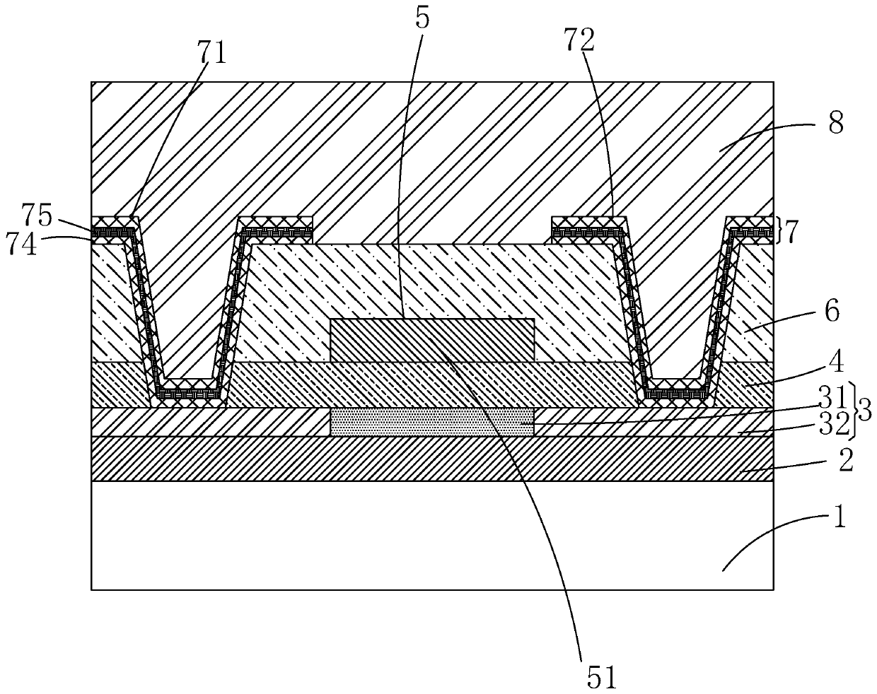
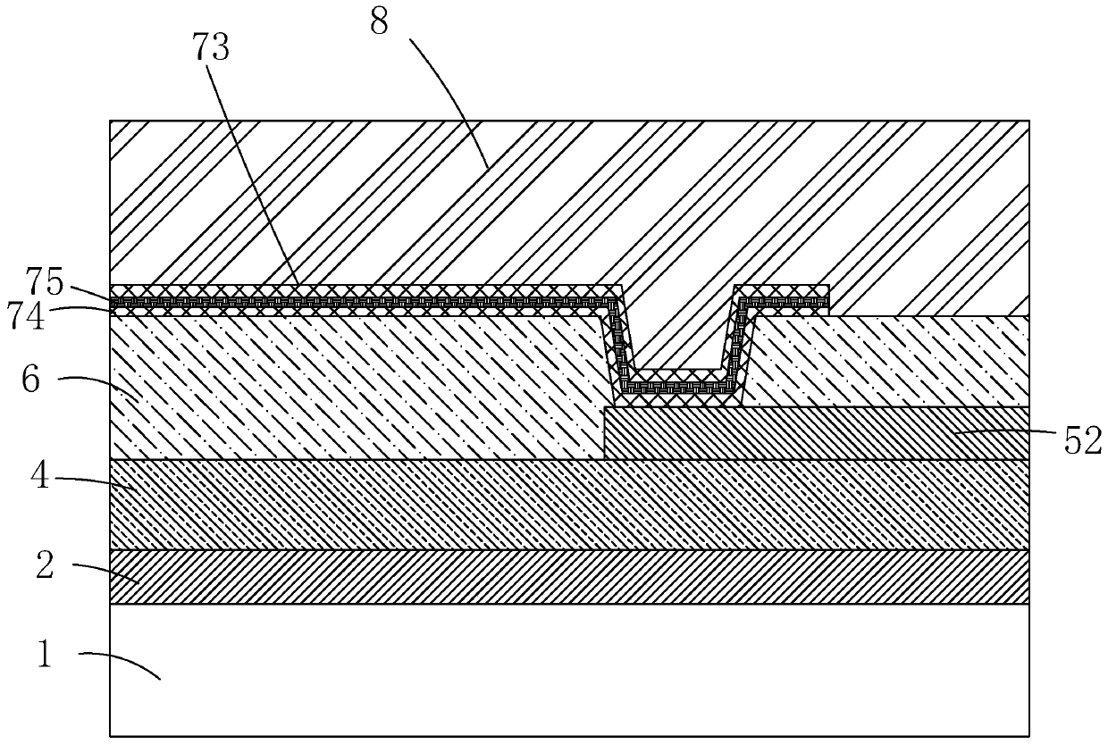
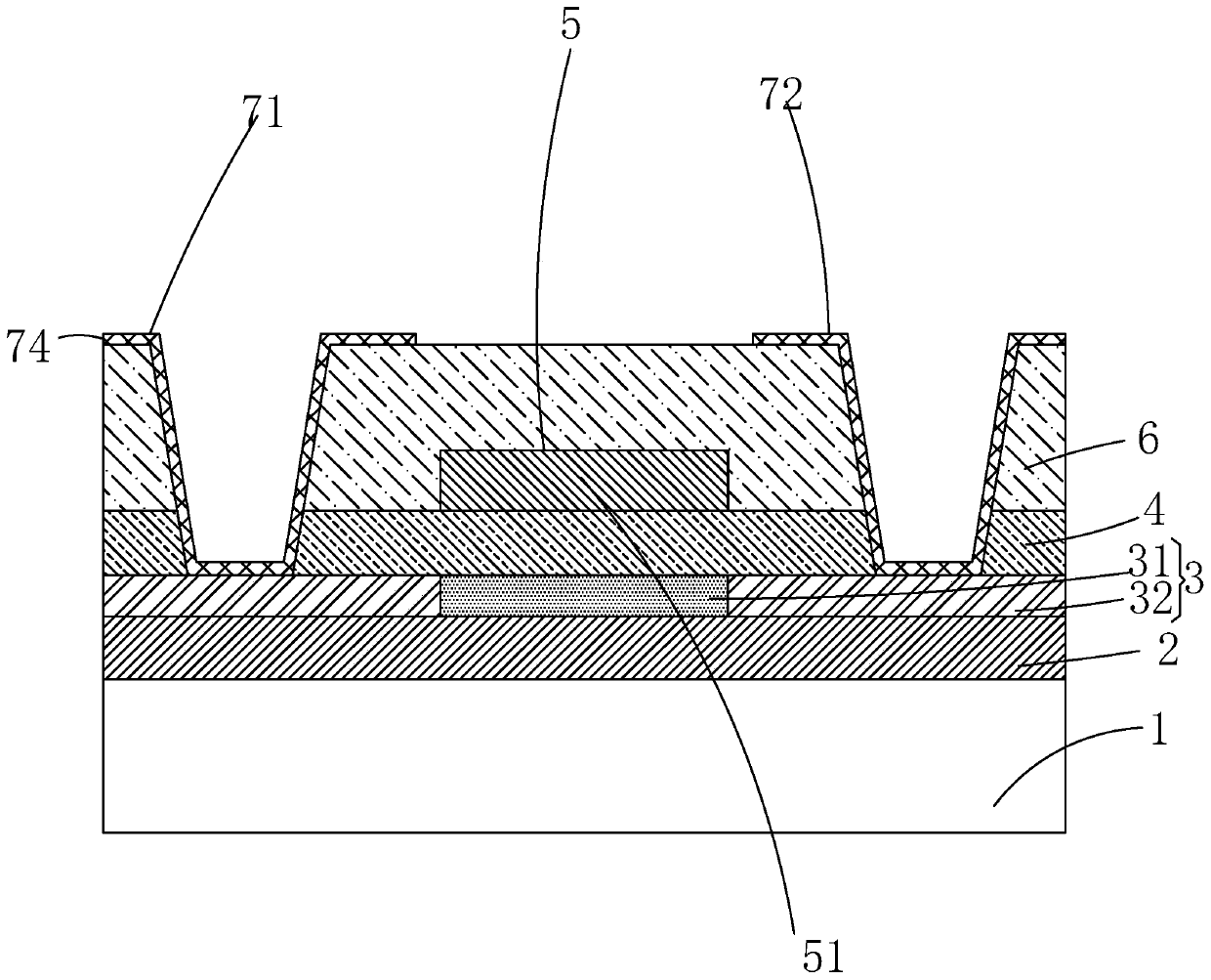
[0035] Step S1, providing an LTPS display panel to be tested, such as figure 1 and figure 2 shown, said figure 1 This is the sectional view of the LTPS display panel to be tested along the direction perpendicular to the gate lines 52, figure 2 This is the sectional view of the LTPS display panel to be tested along the gate line 52. The LTPS display panel to be tested includes: a substrate 1, a buffer layer 2 disposed on the substrate 1, a buffer layer 2 disposed on the buffer The active layer 3 on the layer 2, the gate insulating layer 4 disposed on the active layer 3 and the buff...


PUM


Abstract

The invention provides a method for measuring the TFT electrical property of an LTPS display panel. According to the method, a chemical reagent simultaneously reacts with an organic flat layer and aluminum in a second metal layer, so that the organic flat layer, the aluminum in the second metal layer, and a first metal material positioned between the aluminum and the organic flat layer in the second metal layer are removed, only the first metal material, positioned at one side far away from the organic flat layer, in the second metal layer is reserved, meanwhile, the aluminum in the second metal layer does not need to be reserved when the organic flat layer is removed, so that the measurement deviation for the TFT electrical property caused by the nonuniform etching on the surface of the aluminum in the second metal layer is avoided, the TFT electrical property of the LTPS display panel can be accurately measured, the measurement success rate for the TFT electrical property of the LTPS display panel is promoted, and the yield of the LTPS display panel product is guaranteed.

Description

technical field [0001] The invention relates to the field of display technology, in particular to a method for measuring TFT electrical properties of an LTPS display panel. Background technique [0002] Flat-panel display devices have many advantages such as thin body, power saving, and no radiation, and have been widely used. Existing flat panel display devices mainly include liquid crystal display devices (Liquid Crystal Display, LCD) and organic light emitting diode display devices (Organic Light Emitting Display, OLED). [0003] In flat panel display devices, thin film transistors (Thin Film Transistor, TFT) are generally used as switching elements to control the operation of pixels, or as driving elements to drive pixels. Thin film transistors can generally be classified into two types: amorphous silicon (a-Si) and polycrystalline silicon (poly-Si) according to the nature of the silicon film. Due to the defects of amorphous silicon itself, such as low on-state current...

Claims


Application Information

Patent Timeline
Patent Type & Authority Patents(China)
IPC IPC(8): G09G3/00
CPCG09G3/006
Inventor 孟林
Owner WUHAN CHINA STAR OPTOELECTRONICS TECH CO LTD
Why Eureka
Try Eureka