Pixel driving circuit, driving method thereof and display device

A technology of pixel driving circuit and driving module, applied in static indicators, instruments, etc., can solve the problems of inability to achieve high PPI, uneven display brightness, large pixel pitch PixelPitch, etc., to save the number of settings, reduce the number of settings, cost reduction effect

Inactive Publication Date: 2017-05-31
BOE TECH GRP CO LTD
View PDF6 Cites 4 Cited by
  • Summary
  • Abstract
  • Description
  • Claims
  • Application Information

AI Technical Summary

Problems solved by technology

However, in practical applications, due to reasons such as process and device aging, the threshold voltages of the driving tubes of each pixel driving circuit are not equal, so that the current flowing through each pixel OLED will change relative to the theoretical value. As a result, the display brightness is uneven, which affects the display effect of the entire image
[0004] In order to solve the above problems, the prior art adopts a 6T1C pixel drive circuit with a compensation circuit, but it also has the following technical problems: since a pixel drive circuit can only drive one pixel, and a data line needs to be set, if To drive multiple pixels, multiple pixel drive circuits and multiple data lines need to be set up, and multiple data drive ICs need to be set up at the same time. high cost

Method used


Image

  • Pixel driving circuit, driving method thereof and display device
  • Pixel driving circuit, driving method thereof and display device
  • Pixel driving circuit, driving method thereof and display device

Examples


Embodiment 1

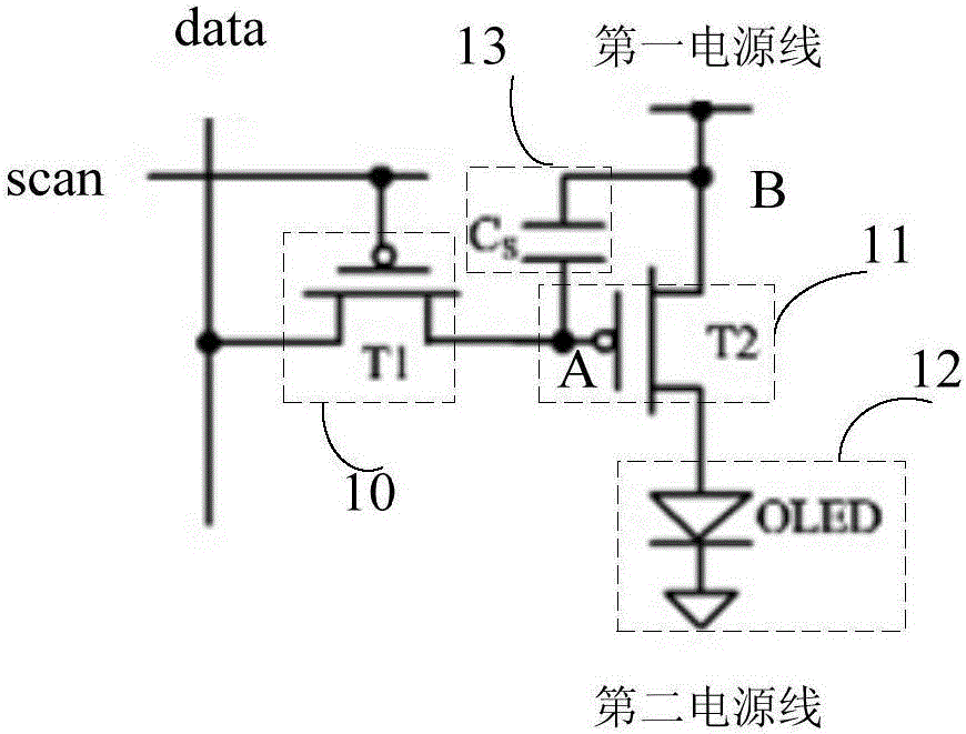
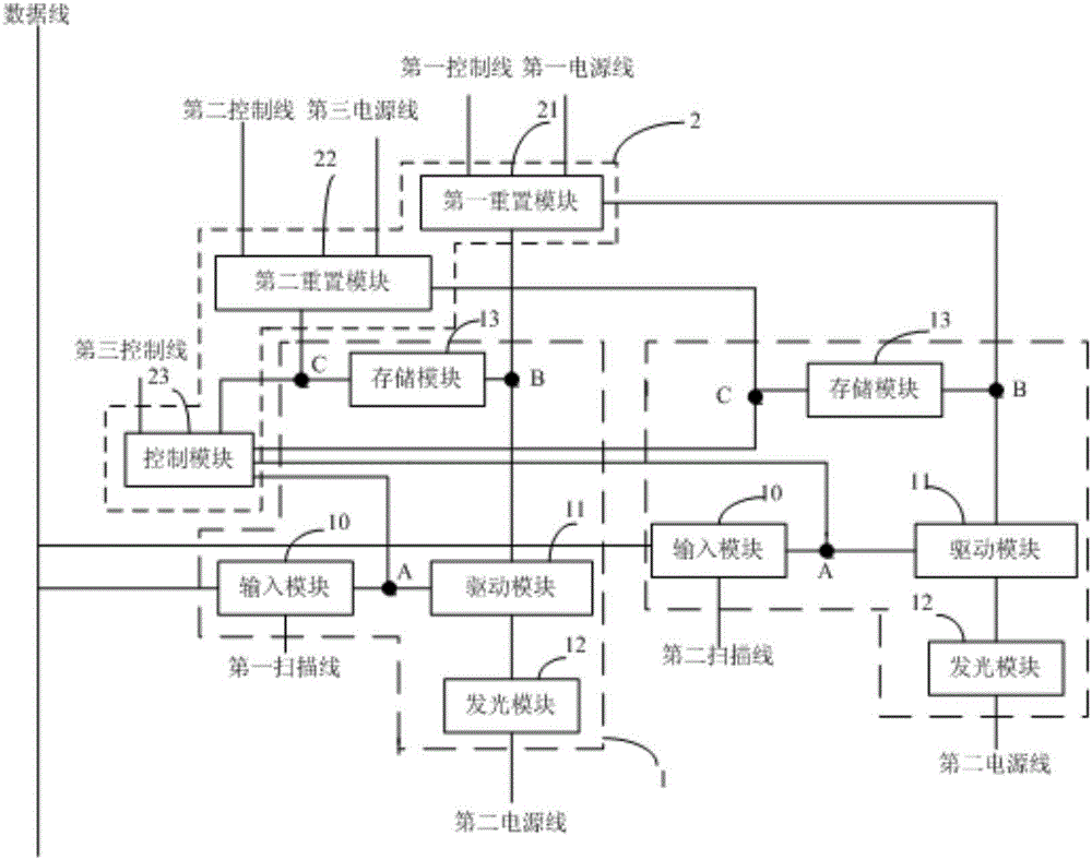
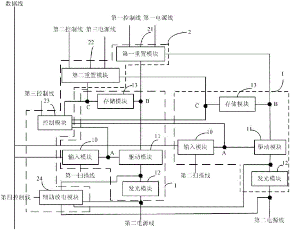
[0055] figure 2 For a schematic block diagram of a pixel driving circuit provided by an embodiment of the present invention, please refer to figure 2 , the pixel driving circuit provided by the embodiment of the present invention includes: a compensation unit and a plurality of light-emitting units 1, figure 2 Taking two light-emitting units 1 as an example to illustrate, of course, the number of light-emitting units 1 in the present invention can also be more than three; a plurality of light-emitting units 1 are connected to the same data line data but are figure 2 The first scan line and the second scan line are connected in one-to-one correspondence, that is, the light-emitting unit 1 is connected to the scan line in a one-to-one correspondence; each light-emitting unit 1 includes: an input module 10, a driving module 11, a light-emitting module 12, and a storage module 13 , a first node A, a second node B and a third node C; the compensation unit 2 includes: a first r...

Embodiment 2

[0088] Based on the same inventive concept, an embodiment of the present invention provides a driving method for the pixel driving circuit provided in the above-mentioned Embodiment 1, including a reset step, a data writing and discharging step, and a compensation lighting step; wherein

[0089] In the reset step, the first reset module provides the signal on the first power line to all the second nodes under the control of the signal on the first control line; the second reset module provides the signal on the second control line The signals on the third power line are provided to all the third nodes under the control of the third node; all the storage modules are charged under the control of the signals on the third node and the second node.

[0090] In the data writing and discharging step, valid signals are sequentially input on a plurality of the scan lines, and the first reset module disconnects the first power line and all the first power lines under the control of the s...

Embodiment 3

[0095] An embodiment of the present invention further provides a display device, and the display device includes the pixel driving circuit provided in Embodiment 1 of the present invention. The principle of solving the problem of the display device is similar to that of the aforementioned pixel driving circuit, so the implementation of the display panel can refer to the implementation of the aforementioned pixel driving circuit, and the repetition is not repeated here.

[0096] During specific implementation, the display device provided by the embodiment of the present invention may be any product or component with display function, such as a mobile phone, a tablet computer, a television, a monitor, a notebook computer, a digital photo frame, and a navigator.


PUM


Abstract

The invention provides a pixel driving circuit. The pixel driving circuit is characterized in that each input module is connected with a data line, a corresponding scanning line and a corresponding first node, and the data line and the first node are connected under the control of the scanning line; a control end of a driving module is connected with a corresponding first node, a first end and a second end are connected with a corresponding second node and a first end of a corresponding light emitting module, and the second node and the first end of the light emitting module are conducted under the control of the first node; a first reset module is connected with a first power line, a first control line and all second nodes, so that the first power line and the second nodes are conducted independently under the control of the first control line; a control module is connected with all first nodes, all third nodes and a third control line, so that the third nodes and the corresponding first nodes are conducted independently under the control of the third control line; a second reset module is connected with a third power line, a second control line and all the third nodes, so that the third power line and the third nodes are conducted under the control of the second control line; a first end and a second end of a memory module are connected with the corresponding second node and the corresponding third node respectively, so that charge and discharge are performed under the control of the second node and the third node, and voltage difference of the second node and the third node is kept when the third node is in suspension joint.

Description

technical field [0001] The invention belongs to the field of display technology, and in particular relates to a pixel driving circuit, a driving method of the pixel driving circuit and a display device. Background technique [0002] Organic Light Emitting Display (OLED) is one of the hot spots in the field of flat panel display research. Compared with liquid crystal display, OLED has the advantages of low energy consumption, low production cost, self-illumination, wide viewing angle and fast response speed. , digital cameras and other display fields OLED has begun to replace the traditional LCD display. Pixel drive circuit design is the core technology content of OLED display, which has important research significance. [0003] Unlike TFT-LCD, which uses stable voltage to control brightness, OLED is current-driven and requires stable current to control light emission. figure 1 For existing pixel driver circuits, see figure 1 , the pixel driving circuit includes a light-em...

Claims


Application Information

Patent Timeline
Patent Type & Authority Applications(China)
IPC IPC(8): G09G3/3208
CPCG09G3/3208
Inventor 杨盛际董学吕敬陈小川王磊刘冬妮卢鹏程付杰岳晗肖丽
Owner BOE TECH GRP CO LTD
Why Eureka
Try Eureka