High-electron-mobility transistor and preparation method thereof
A high electron mobility and transistor technology, applied in the field of microelectronics, can solve the problems of leakage and instability of high electron mobility transistors, and achieve the effects of reducing parasitic capacitance, small leakage and increasing frequency
- Summary
- Abstract
- Description
- Claims
- Application Information
AI Technical Summary
Problems solved by technology
Method used
Image

Examples
Embodiment 1
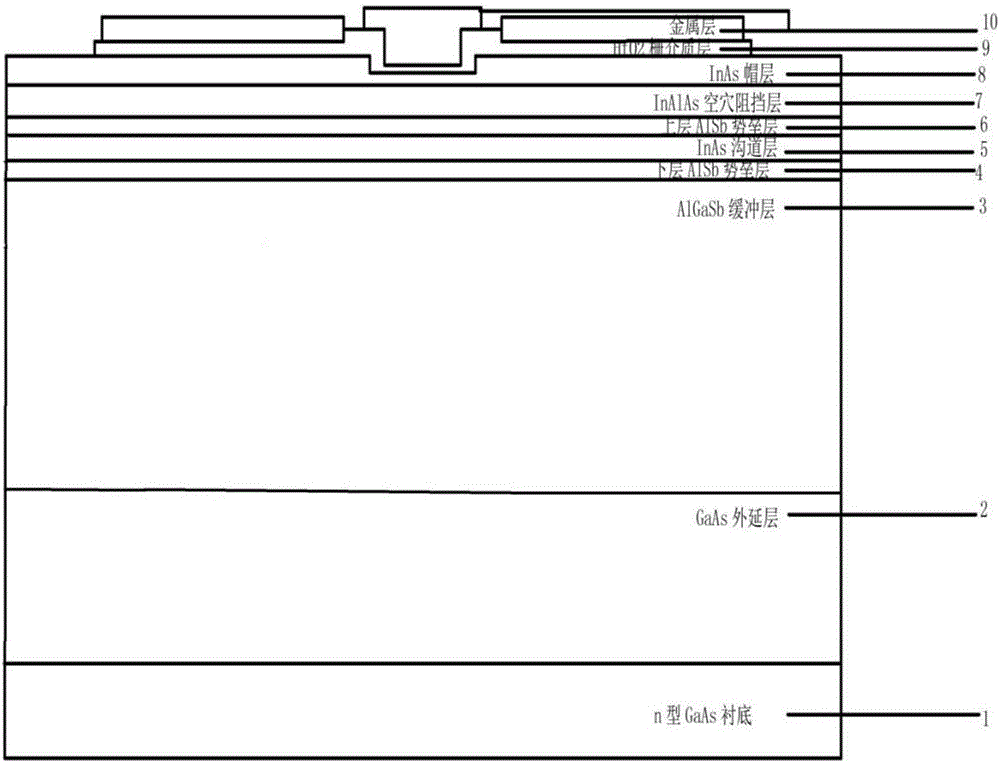
[0016] Embodiment 1 A high electron mobility transistor, which comprises an n-type GaAs substrate 1, a GaAs epitaxial layer 2 with a thickness of 150 nm, an AlGaSb buffer layer 3 with a thickness of 600 nm, and a lower AlSb barrier layer 4 with a thickness of 70 nm, An InAs channel layer 5 with a thickness of 12nm, an upper AlSb barrier layer 6 with a thickness of 5nm, an InAlAs hole blocking layer 7 with a thickness of 6nm, an InAs cap layer 8 with a thickness of 4nm, HfO 2 Gate dielectric layer 9 and metal layer 10, the structure of the high electron mobility transistor is arranged in order from bottom to top: n-type GaAs substrate 1, GaAs epitaxial layer 2 with a thickness of 150 nm, AlGaSb buffer layer 3 with a thickness of 600 nm, A lower AlSb barrier layer 4 with a thickness of 70nm, an InAs channel layer 5 with a thickness of 12nm, an upper AlSb barrier layer 6 with a thickness of 5nm, an InAlAs hole blocking layer 7 with a thickness of 6nm, and an InAs cap layer with a ...
Embodiment 2
[0017] Embodiment 2 A high electron mobility transistor, which comprises an n-type GaAs substrate 1, a GaAs epitaxial layer 2 with a thickness of 150nm, an AlGaSb buffer layer 3 with a thickness of 600nm, and a lower AlSb barrier layer 4 with a thickness of 70nm, The lower AlSb barrier layer 4 is doped with Si at a concentration of 2×10 18 cm -3 ; Thickness is the InAs channel layer 5 of 12nm, and the InAs channel layer 5 is doped with Si and its concentration is 5×10 17 cm -3 , an upper AlSb barrier layer with a thickness of 5nm, in which the elemental ratio of In:Al:As is 1:1:26, an InAlAs hole blocking layer 7 with a thickness of 6nm, an InAs cap layer 8 with a thickness of 4nm, in the InAs cap layer Middle-doped right Si with a doping concentration of 2×10 19 cm -3 , HfO2 gate dielectric layer 9 and metal layer 10, the structure of the high electron mobility transistor is arranged from bottom to top in order of n-type GaAs substrate 1, GaAs epitaxial layer 2 with a thi...
Embodiment 3
[0021] Embodiment 3 The present invention also provides a preparation method for the above-mentioned high electron mobility transistor, which specifically includes the following steps: the first step: cleaning the n-type GaAs semi-insulating substrate sample; specifically including (a) setting the doping concentration to lx 10 18 cm -3 Highly doped n-type 4H-SiC substrate sample in NH 4 OH+H 2 o 2 Soak the sample in the reagent for 10 minutes, take it out and dry it to remove the organic residue on the surface of the sample; (b) use HCl+H on the sample after removing the organic residue on the surface 2 o 2 Soak the sample in the reagent for 10 minutes, take it out and dry it to remove ionic pollutants; (c) soak the sample in 5% HF solution for 3 minutes to remove the surface oxide layer, and then ultrasonically clean it in deionized water for 5 minutes. The second step: put the cleaned sample into the MBE growth chamber, raise the temperature to 680°C in the As atmospher...
PUM
 Abstract
Description
Claims
Application Information
 - R&D Engineer
- R&D Manager
- IP Professional
- Industry Leading Data Capabilities
- Powerful AI technology
- Patent DNA Extraction
Browse by: Latest US Patents, China's latest patents, Technical Efficacy Thesaurus, Application Domain, Technology Topic.
© 2024 PatSnap. All rights reserved.Legal|Privacy policy|Modern Slavery Act Transparency Statement|Sitemap