
Charge reservoir IGBT top structure

a top structure and charge reservoir technology, applied in the field of insulated gate bipolar transistor device structure, can solve the problems of higher turn-off switching loss, difficulty in further improvement of performance, and limitations of conventional igbt device configuration and manufacturing technologies, and achieve the cost of lowering the breakdown voltage vsub>bd/sub>

Active Publication Date: 2015-05-21
ALPHA & OMEGA SEMICON INC
View PDF1 Cites 2 Cited by
  • Summary
  • Abstract
  • Description
  • Claims
  • Application Information

AI Technical Summary

Benefits of technology

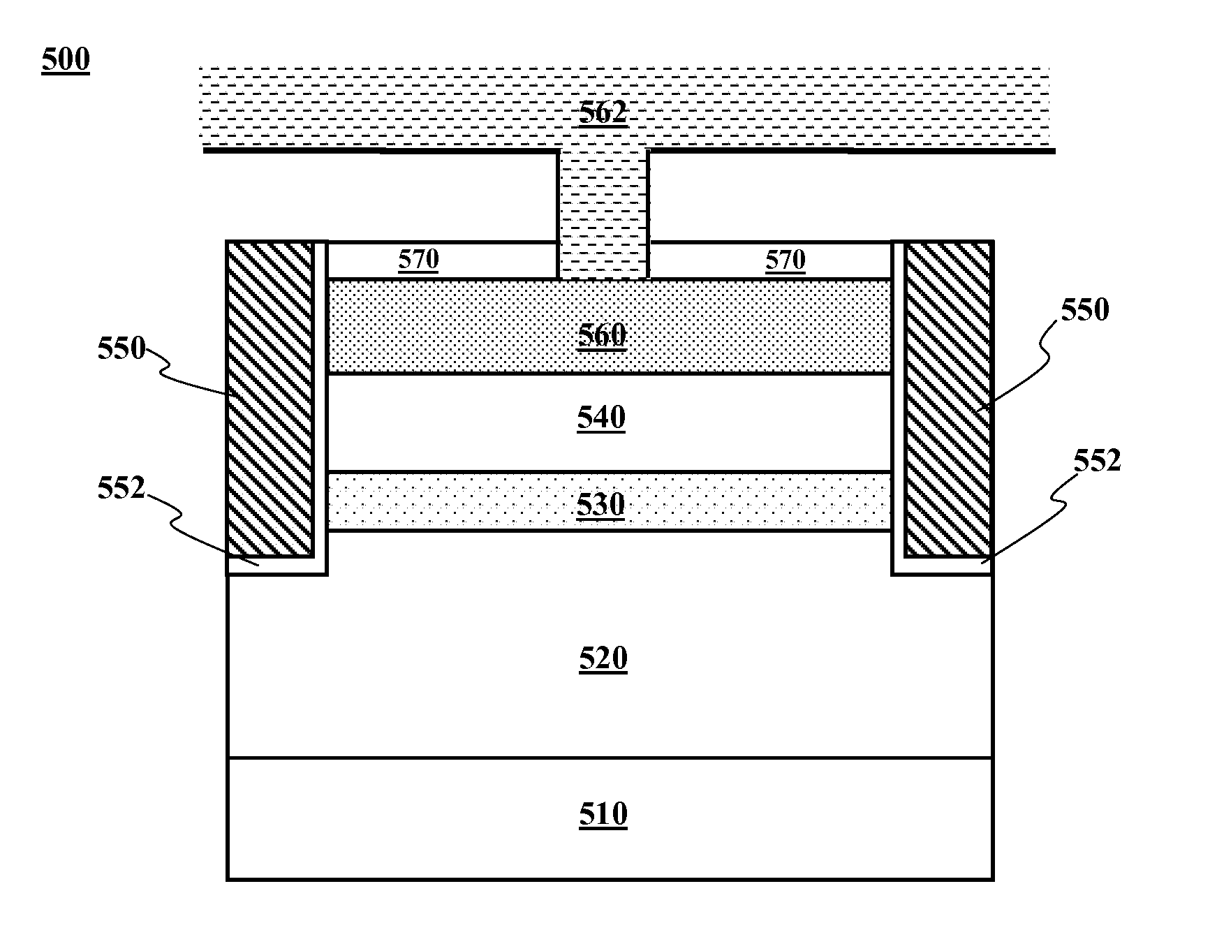
The present disclosure relates to an improved design for IGBT devices. These devices have several limitations in terms of their breakdown voltage and saturation voltage. To overcome these limitations, the present invention introduces a floating P body which isolates the N body and provides a charge balance and an effective electrical field shield. The floating P body helps to lower the breakdown voltage of the device and allows for a higher doping level of the N body without affecting the breakdown voltage. This results in a device with improved performance and stability.

Problems solved by technology

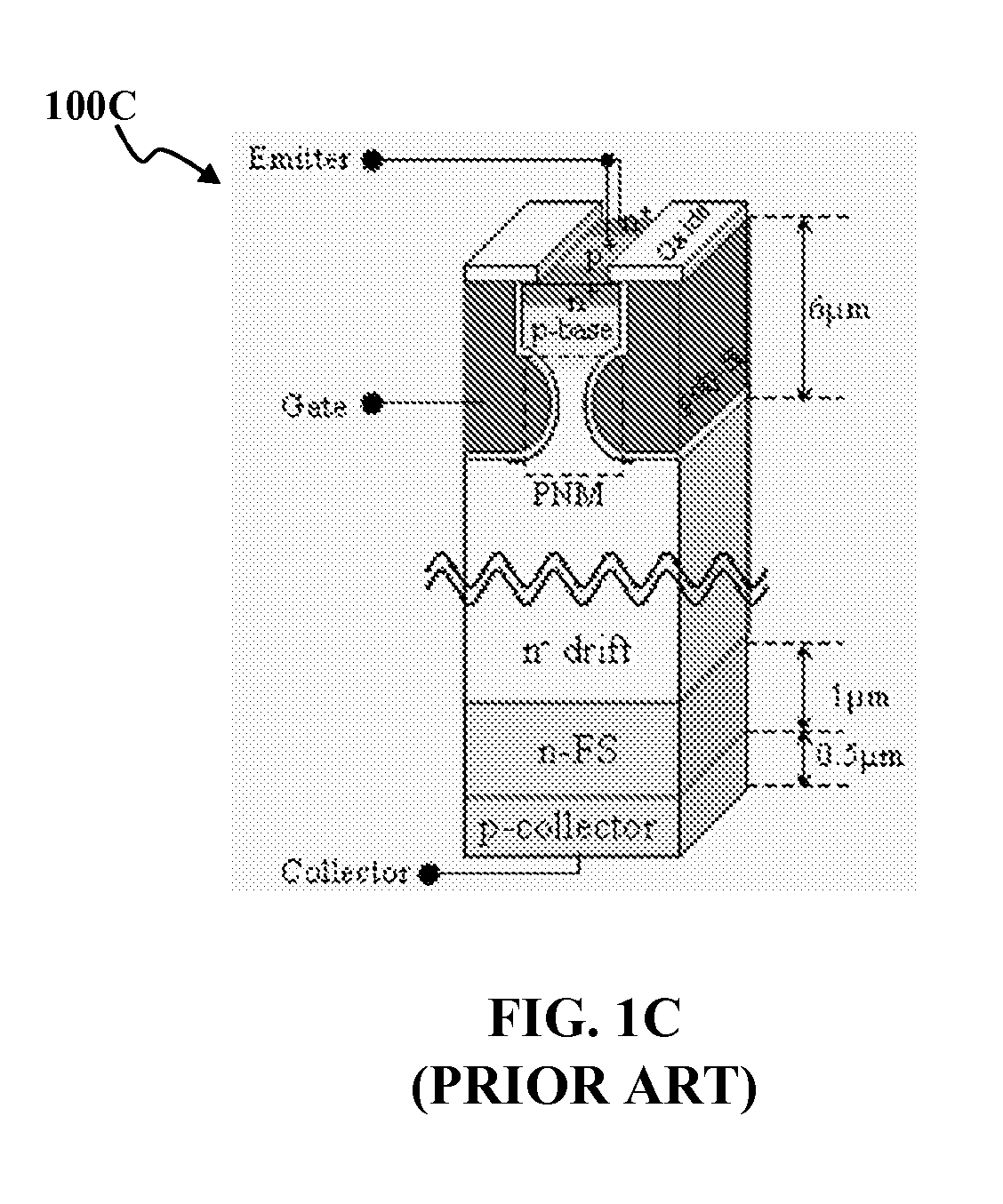
Conventional technologies to configure and manufacture IGBT devices are still confronted with difficulties and limitations to further improvement in performance due to various tradeoffs.
Increased carrier injection would, however, cause higher turn-off switching losses because of energy dissipated in clearing out injected carriers during turn-off.
While an increase on topside injection may improve Vce(SAT), it usually comes at a cost of lowering breakdown voltage VBD.
An IGBT device with a high density of deep trenches may overcome this trade-off, but it is hard to make such device with a high density of small pitch high aspect ratio trenches.
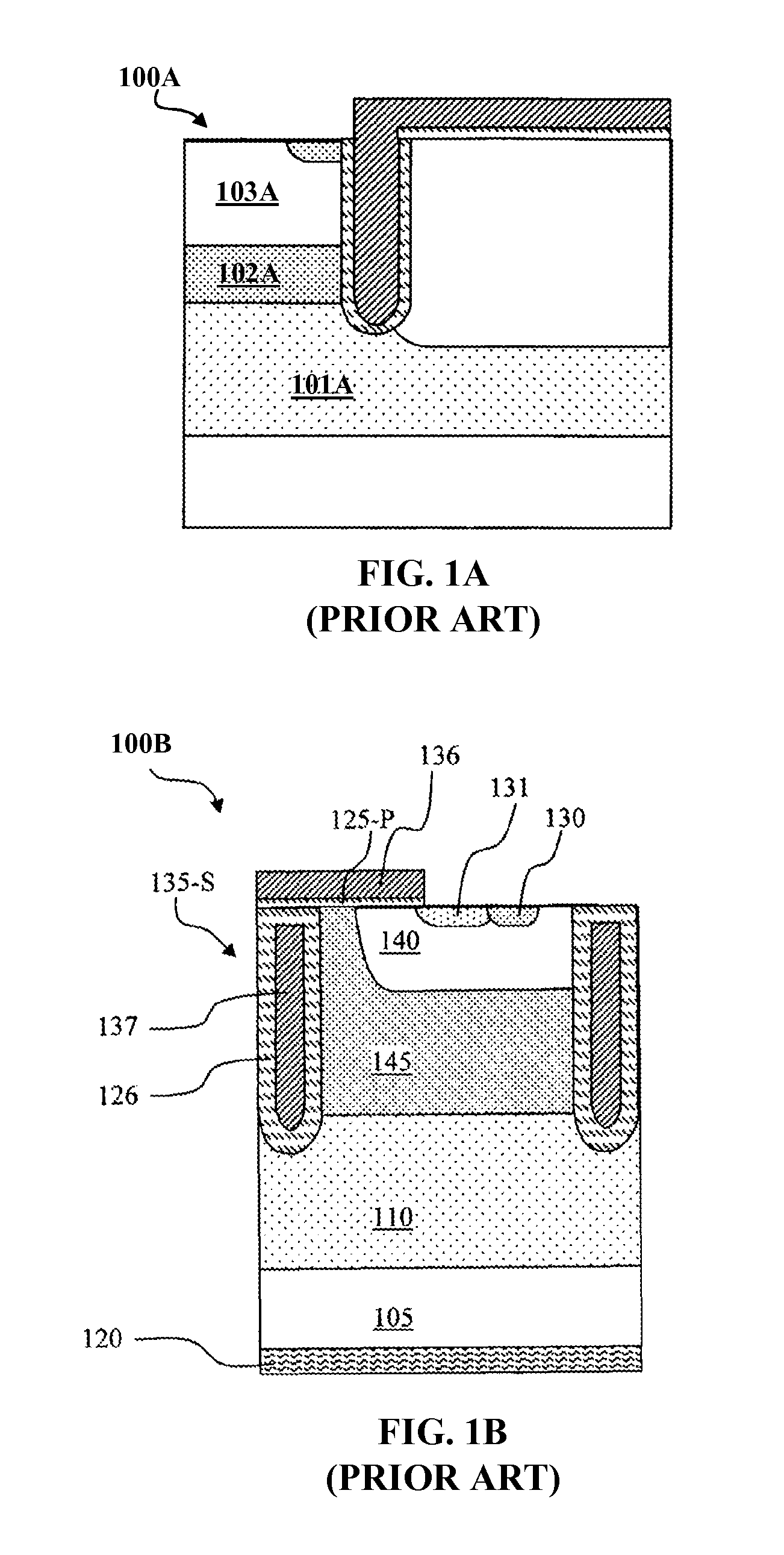
However, such a device has a lower breakdown voltage and has a high Crss capacitance due to the heavily doped N layer 102A.
The high Crss capacitance of the IGBT device may slow down the device switching speed and lead to higher switching energy loss.
However, such a device requires complicated design and process.

Method used


Image

  • Charge reservoir IGBT top structure
  • Charge reservoir IGBT top structure
  • Charge reservoir IGBT top structure

Examples


Embodiment Construction

[0017]Although the following detailed description contains many specific details for the purposes of illustration, anyone of ordinary skill in the art will appreciate that many variations and alterations to the following details are within the scope of the invention. Accordingly, the exemplary embodiments of the invention described below are set forth without any loss of generality to, and without imposing limitations upon, the claimed invention.

[0018]In the following detailed description, reference is made to the accompanying drawings, which form a part hereof, and in which is shown by way of illustration specific embodiments in which the invention may be practiced. In this regard, directional terminology, such as “top,”“bottom,”“front,”“back,”“first,”“second,” etc., is used with reference to the orientation of the figure(s) being described. Because components of embodiments of the present invention can be positioned in a number of different orientations, the directional terminolog...


PUM


Abstract

An IGBT device includes one or more trench gates disposed over a semiconductor substrate and a floating body region of the first conductivity type disposed between two neighboring trench gates and between a semiconductor substrate and a heavily doped top region of the second conductivity type. A body region of the first conductivity type disposed over the top region has a doping concentration higher than that of the floating body region of the first conductivity type. It is emphasized that this abstract is provided to comply with rules requiring an abstract that will allow a searcher or other reader to quickly ascertain the subject matter of the technical disclosure. It is submitted with the understanding that it will not be used to interpret or limit the scope or meaning of the claims.

Description

FIELD OF THE INVENTION[0001]This invention generally relates to semiconductor power devices. More particularly, this invention relates to device structures for insulated gate bipolar transistors (IGBT) and methods for manufacturing thereof.BACKGROUND OF THE INVENTION[0002]An insulated gate bipolar transistor (IGBT) is a semiconductor power device with a compositing structure that combines features of a metal-oxide-semiconductor field effect transistor (MOSFET) and a bipolar junction transistor (BJT). Performance-enhancing features of an IGBT are designed to achieve a higher current density than a MOSFET, and faster and more efficient switching characteristics and better control than a BJT. Additionally, the drift region of the IGBT can be lightly doped for improved blocking ability. Meanwhile, an IGBT device can still have good conductivity because the lightly doped drift region undergoes high level carrier injection from a bottom P collector region resulting in conductivity modulat...

Claims


Application Information

Patent Timeline
Patent Type & Authority Applications(United States)
IPC IPC(8): H01L29/739H01L29/10H01L29/66
CPCH01L29/7397H01L29/1095H01L29/66348H01L29/407H01L29/7395H01L29/0623H01L29/083H01L29/4236H01L29/086H01L29/0696
Inventor HU, JUN
Owner ALPHA & OMEGA SEMICON INC
Learn More