Method of providing a boron doped region in a substrate and a solar cell using such a substrate

a technology of silicon substrate and boron doping, which is applied in the direction of climate sustainability, basic electric elements, final product manufacturing, etc., can solve the problems of expensive processing steps, and achieve the effects of reducing the doping level, high contrast of boron doping level, and high doping level for conta

Active Publication Date: 2015-12-10
NEDERLANDSE ORG VOOR TOEGEPAST-NATUURWETENSCHAPPELIJK ONDERZOEK (TNO)
View PDF15 Cites 3 Cited by
  • Summary
  • Abstract
  • Description
  • Claims
  • Application Information

AI Technical Summary

Benefits of technology

[0004]The present invention seeks to provide a method of providing improved homogenous and selective boron doped regions or emitters having higher efficiencies at reasonable cost.
[0015]The annealing of deposited undoped silicon oxide pulls out boron atoms from the emitter, thus reducing the doping level. In the case of a selective emitter embodiment, annealing of the selectively remaining boron doping source keeps the high doping level for contacting. As a result, a selective emitter is obtained in the substrate having a high contrast of the boron doping level.

Problems solved by technology

This however, requires costly processing steps.

Method used


Image

  • Method of providing a boron doped region in a substrate and a solar cell using such a substrate
  • Method of providing a boron doped region in a substrate and a solar cell using such a substrate
  • Method of providing a boron doped region in a substrate and a solar cell using such a substrate

Examples


Embodiment Construction

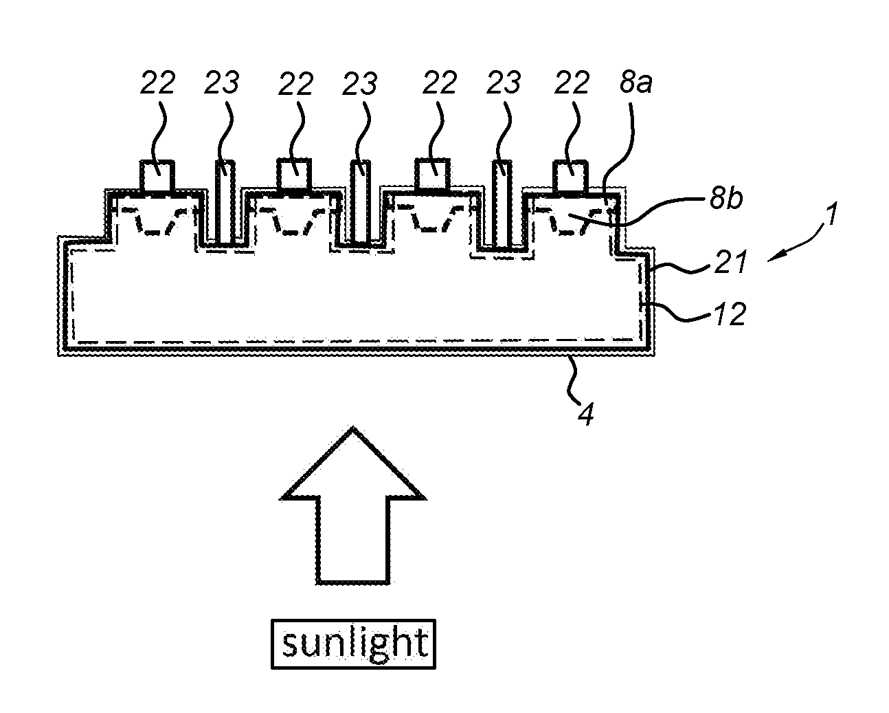
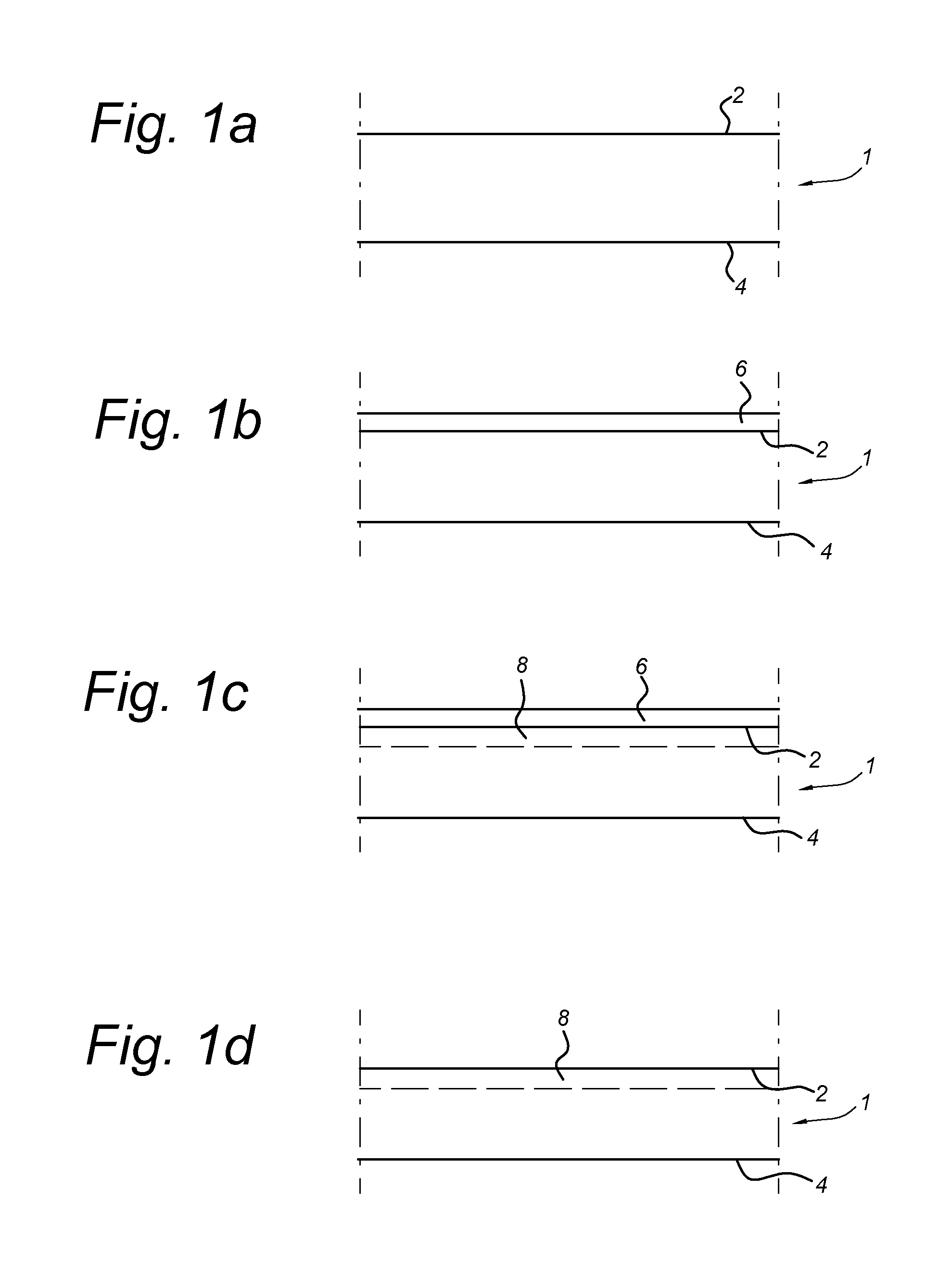
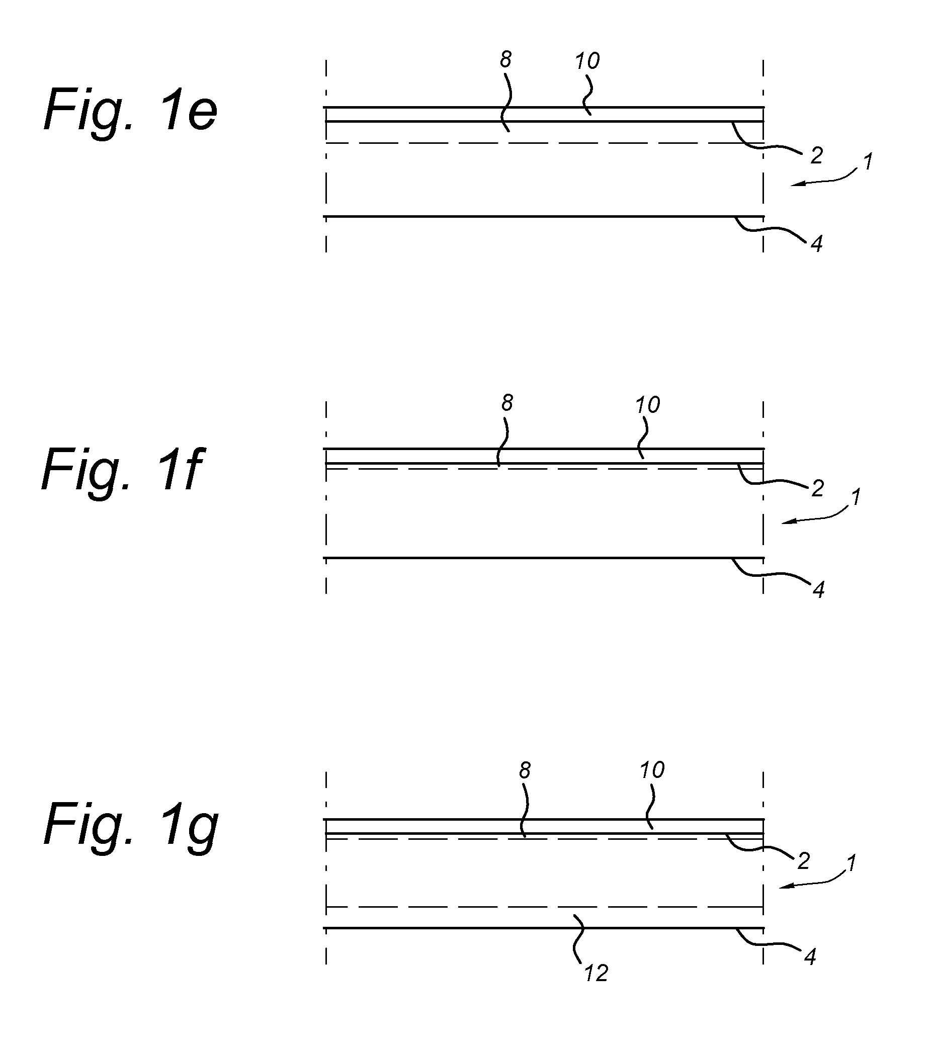
[0022]According to the present invention, FIG. 1a shows a silicon substrate 1 to be provided with a boron-doped region, more particularly a homogenous or selective boron-doped emitter, which is specifically used in solar (photo-voltaic) cells. The substrate 1 comprises a first surface 2 and a second surface 4. The first surface 2 may be referred to as the front side and the second surface 4 may be referred to as the back side. In an embodiment, the silicon substrate 1 is a p-type substrate 1. In a further embodiment, the substrate 1 is a n-type substrate 1.

[0023]The substrate 1 defined above and depicted in FIG. 1a is subsequently subjected to processing steps of an embodiment of the method of the present invention for providing a boron-doped region 8 in a silicon substrate 1, wherein labels such as (a), (b), (c), . . . etc. will be used to label and conveniently refer to the functional processing steps of the method.

[0024]Depicted in FIG. 1b, the method embodiment of the present in...


PUM

PropertyMeasurementUnit
temperatureaaaaaaaaaa

Abstract

Method of providing a boron doped region (8, 8a, 8b) in a silicon substrate (1), includes the steps of: (a) depositing a boron doping source (6) over a first surface (2) of the substrate (1); (b) annealing the substrate (1) for diffusing boron from the boron doping source (6) into the first surface (2), thereby yielding a boron doped region; (c) removing the boron doping source (6) from at least part of the first surface (2); (d) depositing undoped silicon oxide (10) over the first surface (2); and (e) annealing the substrate (1) for lowering a peak concentration of boron in the boron doped region (8, 8a) through boron absorption by the undoped silicon oxide. The silicon oxide (10) acts as a boron absorber to obtain the desired concentration of the boron doped region (8).

Description

FIELD OF THE INVENTION[0001]The present invention relates to a method of providing a boron doped region in a silicon substrate.PRIOR ART[0002]U.S. Pat. No. 5,928,438 (Salami et al.) discloses a solar cell with a selective (boron) emitter. The solar cell comprises a semiconducting substrate having first and second surfaces, a first plurality of emitter regions formed in one of the first and second surfaces with a relatively low dopant concentration, a second plurality of emitter regions formed in said one of the first and second surfaces to a substantially greater depth than the first plurality of regions preferably with a relatively higher dopant concentration than the first plurality of regions. The semiconductor substrate preferably comprises n-type doped silicon, and the first plurality of emitter regions are preferably formed using a p+ type dopant material, such as boron. The second plurality of emitter regions is preferably formed from a p+ type dopant material comprising eith...

Claims


Application Information

Patent Timeline
Patent Type & Authority Applications(United States)
IPC IPC(8): H01L31/065H01L31/18
CPCH01L31/065H01L31/1868H01L31/1864H01L31/1804H01L21/2255H01L21/324H01L31/03529H01L31/068Y02E10/547Y02P70/50
Inventor KOMATSU, YUJIANKER, JOHNBARTON, PAUL CORNELISROMIJN, INGRID GERDINA
Owner NEDERLANDSE ORG VOOR TOEGEPAST-NATUURWETENSCHAPPELIJK ONDERZOEK (TNO)
Why Eureka
Try Eureka