Backside illuminated solid-state imaging device

a solid-state imaging and backside illumination technology, which is applied in the direction of color television, television systems, radio control devices, etc., can solve the problems of abnormal imaging state for a while, unbalanced potential distribution of imaging regions where photodiodes are disposed, and generated dark current noise, which may be a problem in solid-state imaging devices, etc., to achieve the effect of lowering the grounding resistance of a high-concentration p-layer

Inactive Publication Date: 2008-09-11
FUJIFILM CORP
View PDF3 Cites 43 Cited by
  • Summary
  • Abstract
  • Description
  • Claims
  • Application Information

AI Technical Summary

Benefits of technology

[0016]An object of an illustrative, non-limiting embodiment of the invention is to provide a backside illuminated solid-state imaging device, which has a structure for preventing unwanted electrons that are generated in a region other than an imaging region, and that become a dark current or noise, from entering into a signal charge accumulating region, and which has a structure for lowering the grounding resistance of a high-concentration p-layer of the backside surface.

Problems solved by technology

Dark current noise, which may be a problem in solid-state imaging devices, is generated in a depletion layer.
When the resistance for swept holes is high, the potential distribution of an imaging region where the photodiode is disposed becomes unbalanced, and characteristic differences are produced between center pixels and peripheral pixels in an effective imaging region.
Therefore, the sweeping process requires a time period, and there occurs a phenomenon that an abnormal imaging state continues for a while.
However, it is difficult to uniformly embed the metal into the through holes having a depth of 5 to 10 μm) and hence the production cost of a backside illuminated solid-state imaging device is increased.
Also, the manner how unwanted electrons generated in the vicinity of the imaging region are blocked from entering the imaging region is a problem in an image sensor of the backside illuminated type which employs a p-type semiconductor substrate.

Method used


Image

  • Backside illuminated solid-state imaging device
  • Backside illuminated solid-state imaging device
  • Backside illuminated solid-state imaging device

Examples


Embodiment Construction

[0075]Although the invention will be described below with reference to the exemplary embodiment thereof, the following exemplary embodiment and its modification do not restrict the invention.

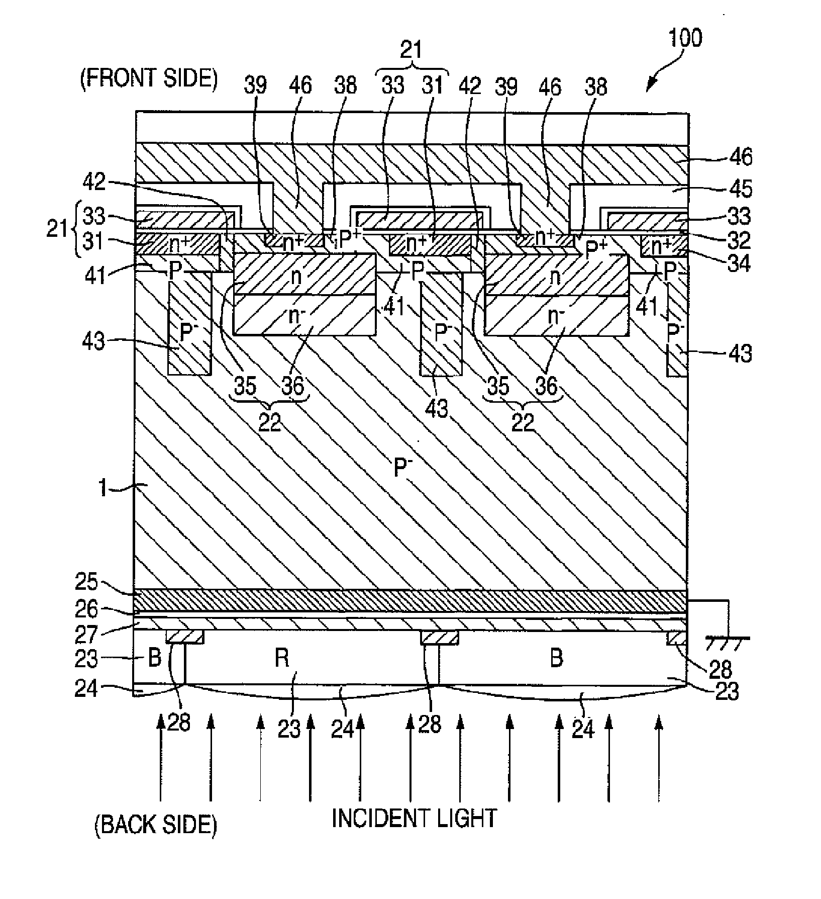
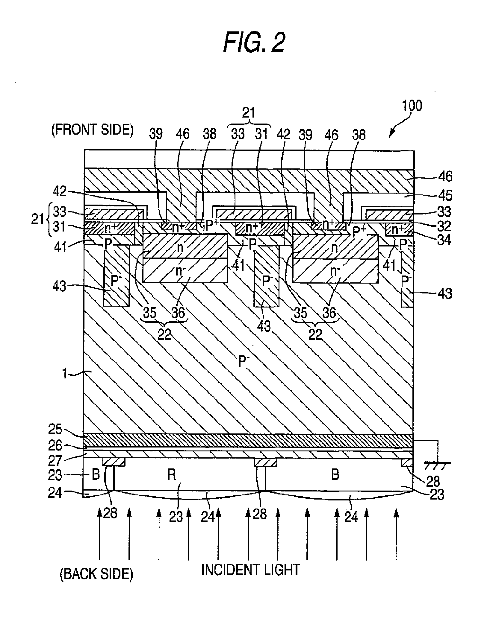
[0076]According to an exemplary embodiment of the invention, unwanted electrons which are generated in a peripheral portion of the substrate are promptly discarded through the n-well region, and holes which are generated inside the substrate are promptly discarded to the outside through the high-concentration p-layer on the back side. Therefore, a highly sensitive object image can be taken at a high S / N ratio.

[0077]Hereinafter, exemplary embodiments of the invention will be described with reference to the accompanying drawings.

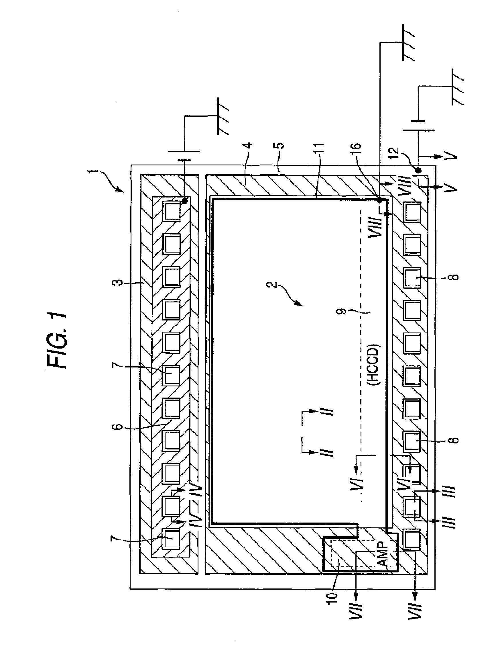
[0078]FIG. 1 is a plan view of a backside illuminated solid-state imaging device of an exemplary embodiment of the invention, as seen from the front side. A semiconductor substrate 1 forming the backside illuminated solid-state imaging device of the embodiment is of the p ...


PUM


Abstract

A backside illuminated solid-state imaging device is provided and includes: a p-type semiconductor substrate; an imaging region that receives a subject light through a back side of the p-type semiconductor substrate to accumulate a signal corresponding to an amount of the received light; a signal reading element disposed in a front side of the p-type semiconductor substrate, the signal reading element reading out the signal from the imaging region; and an n-well region disposed in the front side of the p-type semiconductor substrate and in a periphery of the imaging region, the n-well region being biased to a positive voltage.

Description

[0001]This application is based on and claims priority under 35 U.S.C. § 119 from Japanese Patent Application No. 2007-40558 filed Feb. 21, 2007, the entire disclosure of which is herein incorporated by reference.BACKGROUND OF THE INVENTION[0002]1. Field of the Invention[0003]The present invention relates to a backside illuminated solid-state imaging device, and particularly to a backside illuminated solid-state imaging device having a structure suitable for suppressing dark current noise from mixing to signal charges.[0004]2. Description of Related Art[0005]Solid-state imaging devices such as a CMOS image sensor and a CCD image sensor are classified into the front side illuminated type and the backside illuminated type. The front side illuminated type has a structure in which incident light from an object is received by the same surface as one surface side (hereinafter, this face is referred to as “front side”) of a semiconductor substrate where a signal reading circuit (in the cas...

Claims


Application Information

Patent Timeline
Patent Type & Authority Applications(United States)
IPC IPC(8): H01L31/103H01L27/148H04N5/335H04N5/361H04N5/369H04N5/372H04N5/374
CPCH01L27/14812H01L27/1464H01L27/14837
Inventor UYA, SHINJI
Owner FUJIFILM CORP
Why Eureka
Try Eureka