Methods of manufacturing synthetic diamond material by microwave plasma enhanced chemical vapor deposition from a microwave generator and gas inlet(s) disposed opposite the growth surface area

a technology of microwave plasma and synthetic diamond, which is applied in the direction of crystal growth process, polycrystalline material growth, chemically reactive gas, etc., can solve the problems of high level of boron incorporation into high quality single crystal cvd diamond material formed using microwave plasma, and achieve high purity, high quality, and reliable and consistent processing

Active Publication Date: 2017-05-02
ELEMENT SIX LTD
View PDF141 Cites 2 Cited by
  • Summary
  • Abstract
  • Description
  • Claims
  • Application Information

AI Technical Summary

Benefits of technology

[0030]The aforementioned method may be utilized to grow a large synthetic polycrystalline CVD diamond wafer having a substantially uniform concentration of dopant throughout the wafer or for growing a larger number of single crystal diamonds grown in a single growth run, the plurality of single crystal diamonds having substantially the same dopant concentration. Further still, the method can be utilized to achieving very high levels of doping (e.g. equal to or greater than 2×1020 cm−3) while maintaining good growth rates and good material quality. When uniform doping over large areas is desired, the provision of multiple gas inlet nozzles is preferred. However, when a high level of doping over a relatively small area is required a single gas inlet nozzle may be utilized.
[0034]Embodiments of the present invention use gas flow to control incorporation of dopants such as nitrogen, boron, silicon, phosphorous, lithium and beryllium. Embodiments may also control the concentration and distribution of other defects such as dangling bonds and vacancy clusters. Particularly useful embodiments use gas flow to control the concentration and distribution of boron in synthetic CVD diamond material to meet the needs previously described in the background section of this specification. For example: free-standing polycrystalline diamond wafers which can be reliably and consistently processed using electric discharge machining (EDM) methods, e.g. to form mechanical tool and wear parts; free-standing polycrystalline diamond wafers with consistent and uniform conduction characteristics for use as electrodes, e.g. in water treatment and ozone generation applications; highly boron doped, uniform, high quality single crystal diamond components for use in sensing and electronic applications, e.g. electrochemical sensing applications which require very high boron concentrations and electronic components such as diamond diode and transistor structures; gems having a reliable, uniform, consistent, and reproducible colour, e.g. blue boron doped gems and colourless or near colourless gems formed by co-doping using boron and another dopant such as nitrogen; and quantum grade synthetic diamond material comprising a uniform distribution of nitrogen dopant in the form of nitrogen-vacancy (NV−) defects. Further embodiments enable the formation of doped layers which have high purity, well defined interfaces with adjacent undoped layers within a synthetic single crystal CVD diamond.

Problems solved by technology

Previously, while such levels of boron incorporation were possible in thin, lower quality single crystal films and polycrystalline diamond material, such a high level of boron incorporation into high quality single crystal CVD diamond material formed using a microwave plasma, particularly using a substrate having a desirable crystallographic orientation for high quality single crystal CVD diamond growth, was not achievable.

Method used


Image

  • Methods of manufacturing synthetic diamond material by microwave plasma enhanced chemical vapor deposition from a microwave generator and gas inlet(s) disposed opposite the growth surface area
  • Methods of manufacturing synthetic diamond material by microwave plasma enhanced chemical vapor deposition from a microwave generator and gas inlet(s) disposed opposite the growth surface area
  • Methods of manufacturing synthetic diamond material by microwave plasma enhanced chemical vapor deposition from a microwave generator and gas inlet(s) disposed opposite the growth surface area

Examples


Embodiment Construction

Reactor Hardware and Gas Inlet Configurations

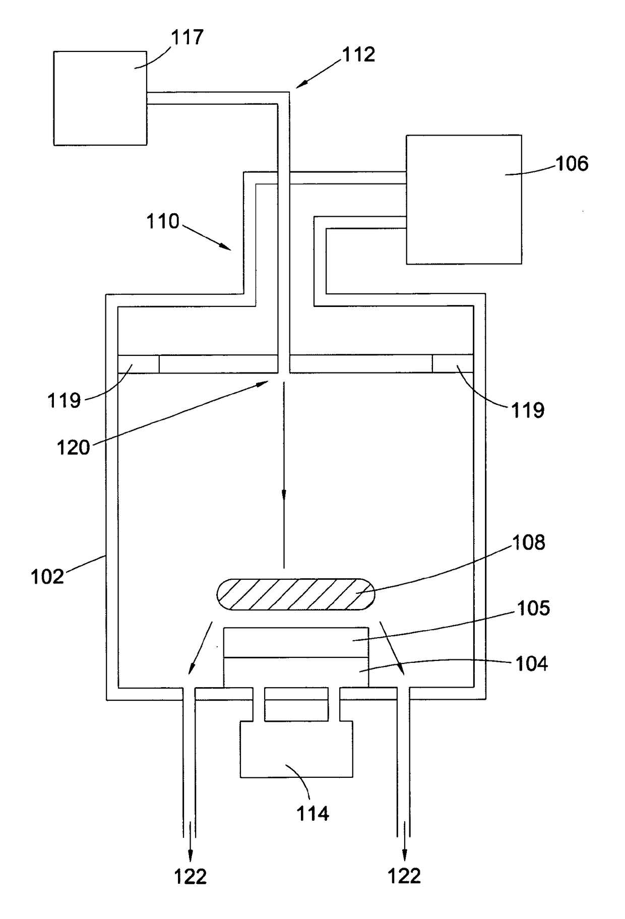
[0050]FIG. 1 shows a cross-sectional view of a microwave plasma reactor configured to deposit a synthetic CVD diamond film using a single axially disposed gas inlet nozzle arranged to inject process gases towards a growth surface of a substrate as a directed jet of high velocity process gas.

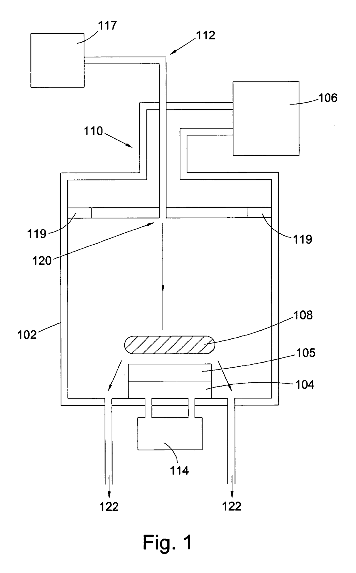
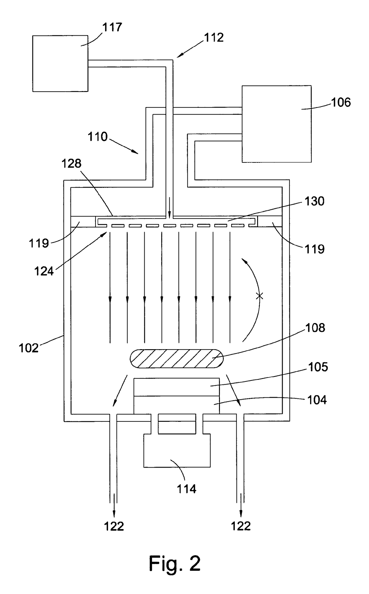
[0051]The microwave plasma reactor comprises the following basic components: a plasma chamber 102; a substrate holder 104 disposed in the plasma chamber for holding a substrate 105; a microwave generator 106 for forming a plasma 108 within the plasma chamber 102; a microwave coupling configuration 110 for feeding microwaves from the microwave generator 106 into the plasma chamber 102 via a coaxial waveguide and through an annular dielectric window 119; a gas flow system 112, 122 for feeding process gases into the plasma chamber 102 and removing them therefrom; and a substrate coolant system 114 for controlling the temperature of a substrate 105.

[0052]T...


PUM

PropertyMeasurementUnit
Reynolds numberaaaaaaaaaa
outlet diameteraaaaaaaaaa

Abstract

Disclosed herein are methods of manufacturing synthetic CVD diamond material including orienting and controlling process gas flow in a microwave plasma reactor to improve performance. The microwave plasma reactor includes a gas flow system with a gas inlet comprising one or more gas inlet nozzles disposed opposite the growth surface area and configured to inject process gases towards the growth surface area. The method comprises injecting process gases towards the growth surface area at a total gas flow rate equal to or greater than 500 standard cm3 per minute wherein the process gases are injected into the plasma chamber through the one or more gas inlet nozzles with a Reynolds number in a range 1 to 100.

Description

FIELD OF INVENTION[0001]The present invention relates to a method of controlling the concentration and uniformity of dopants in synthetic diamond material manufactured using a chemical vapour deposition (CVD) technique.BACKGROUND OF INVENTION[0002]CVD processes for manufacture of synthetic diamond material are now well known in the art. Useful background information relating to the chemical vapour deposition of diamond materials may be found in a special issue of the Journal of Physics: Condensed Matter, Vol. 21, No. 36 (2009) which is dedicated to diamond related technology. For example, the review article by R. S Balmer et al. gives a comprehensive overview of CVD diamond materials, technology and applications (see “Chemical vapour deposition synthetic diamond: materials, technology and applications” J. Phys.: Condensed Matter, Vol. 21, No. 36 (2009) 364221).[0003]Being in the region where diamond is metastable compared to graphite, synthesis of diamond under CVD conditions is dri...

Claims


Application Information

Patent Timeline
Patent Type & Authority Patents(United States)
IPC IPC(8): C30B25/14C30B25/16C30B25/02H01J37/32C30B29/04C23C16/27
CPCC30B25/14C01B31/06C23C16/274C23C16/278C30B25/02C30B25/165C30B29/04H01J37/32192H01J37/32449C01B32/25C01B32/26H01J37/32
Inventor COE, STEVEN EDWARDWILMAN, JONATHAN JAMESTWITCHEN, DANIEL JAMESSCARSBROOK, GEOFFREY ALANBRANDON, JOHN ROBERTWORT, CHRISTOPHER JOHN HOWARDMARKHAM, MATTHEW LEE
Owner ELEMENT SIX LTD
Why Eureka
Try Eureka