Luminous device and manufacturing method thereof

A technology for a light-emitting device and an organic light-emitting layer, which is applied in the directions of manufacturing/processing of organic light-emitting devices, organic light-emitting devices, organic light-emitting device structures, etc., can solve the problems of high manufacturing cost, many manufacturing process steps, etc. The effect of reducing manufacturing costs

Inactive Publication Date: 2017-05-31
GUAN YEOLIGHT TECH CO LTD
View PDF5 Cites 5 Cited by
  • Summary
  • Abstract
  • Description
  • Claims
  • Application Information

AI Technical Summary

Problems solved by technology

[0004] In view of this, an embodiment of the present invention provides a light-emitting device and a manufacturing method thereof, so as to solve the problems of many manufacturing steps and high manufacturing cost of the light-emitting device in the prior art

Method used


Image

  • Luminous device and manufacturing method thereof
  • Luminous device and manufacturing method thereof
  • Luminous device and manufacturing method thereof

Examples


Embodiment Construction

[0025] In order to make the purpose, technical solutions and advantages of the embodiments of the present invention clearer, the technical solutions in the embodiments of the present invention will be clearly and completely described below in conjunction with the drawings in the embodiments of the present invention. Obviously, the described embodiments It is a part of embodiments of the present invention, but not all embodiments. Based on the embodiments of the present invention, all other embodiments obtained by those skilled in the art without creative efforts fall within the protection scope of the present invention.

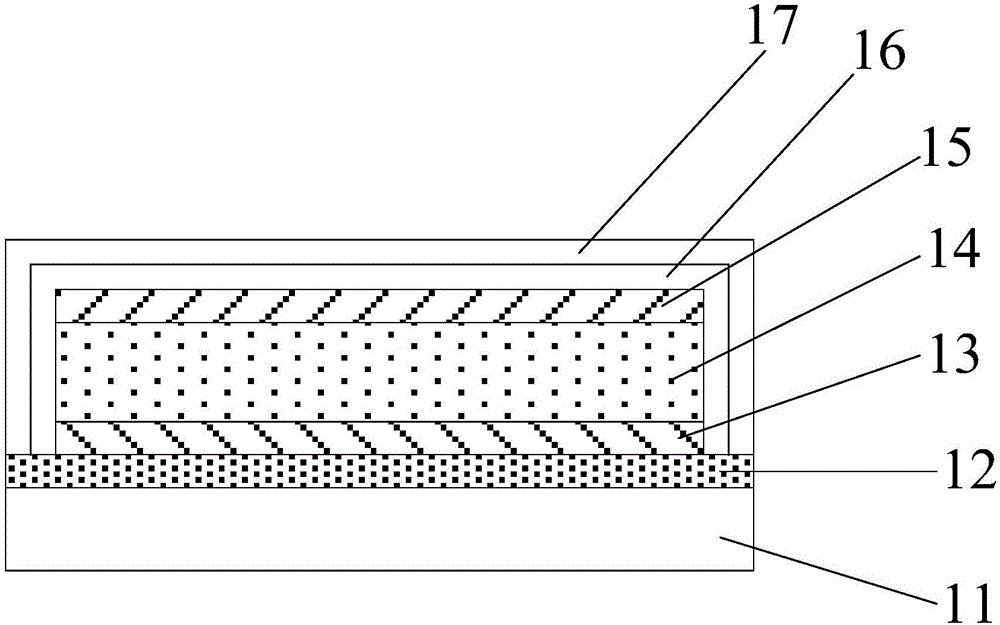
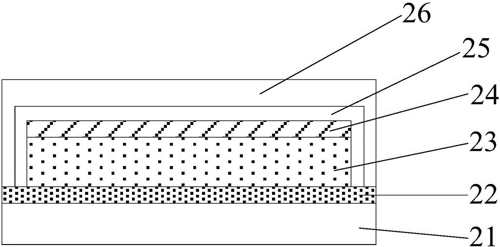
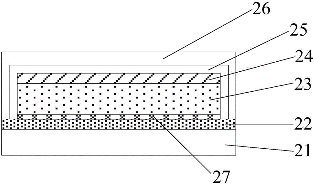
[0026] figure 2 A schematic diagram of a light emitting device according to an embodiment of the present invention, such as figure 2 As shown, the light-emitting device may include a substrate 21, a conductive hydrophobic layer 22, an organic light-emitting layer 23, an electrode layer 24, and a passivation layer 25, wherein the conductive hydrophobic laye...


PUM


Abstract

The invention discloses a luminous device and a manufacturing method thereof, wherein the luminous device comprises a base plate, a conducting hydrophobic layer, an organic luminous layer, an electrode layer and a passivation layer, wherein the conducting hydrophobic layer is arranged on the base plate; the organic luminous layer is arranged on the conducting hydrophobic layer; the electrode layer is arranged on the organic luminous layer; the passivation layer is arranged on the electrode layer so as to at least cover the organic luminous layer and the electrode layer. Therefore the conducting hydrophobic layer is arranged between the base plate and the organic luminous layer; meanwhile, an effect of preventing water vapor and oxygen from entering the luminous device and the electrode is achieved; the process steps of additionally installing the blocking layer can be omitted, so that the manufacturing technical steps of the luminous device can be reduced; the manufacturing cost of the luminous device is reduced.

Description

technical field [0001] The invention relates to the technical field of semiconductors, in particular to a light emitting device and a manufacturing method thereof. Background technique [0002] With the continuous development of display technology, light-emitting devices such as organic light-emitting diodes (OLED, Organic Light-Emitting Diode) have been widely used due to their advantages of low energy consumption, light weight, and thin thickness. Bendable properties. [0003] However, water vapor and oxygen are easy to penetrate the substrate and enter the interior of the light-emitting device, thereby affecting the service life of the light-emitting device. Compared with rigid substrates such as glass, flexible substrates are more permeable to water vapor and oxygen. In order to solve this problem, such as figure 1 As shown, the existing OLED light-emitting device usually sets a barrier layer 12 between the substrate 11 and the light-emitting element, and sets an enca...

Claims


Application Information

Patent Timeline
Patent Type & Authority Applications(China)
IPC IPC(8): H01L51/52H01L51/56
CPCH10K50/80H10K50/805H10K50/84H10K2102/301H10K2102/302H10K71/00
Inventor 郭立雪朱映光冯建斌谢静胡永岚
Owner GUAN YEOLIGHT TECH CO LTD
Why Eureka
Try Eureka