A built-in self-test design method for multiple embedded memories on a single chip

A technology of embedded memory and built-in self-test, which is applied in static memory, instruments, etc., can solve the problems of reduced scan test coverage, loss of scan test coverage, and excessively long windings, etc., to improve the overall scan test coverage , Conducive to timing convergence, reduce the effect of circuit power consumption

Active Publication Date: 2020-02-21
BEIJING MXTRONICS CORP +1
View PDF8 Cites 0 Cited by
  • Summary
  • Abstract
  • Description
  • Claims
  • Application Information

AI Technical Summary

Problems solved by technology

[0003] Since the number of integrated memories in previous chips is not very large, and the memory test logic itself will occupy a certain area and power consumption, the traditional method is to use a controller to perform the MBIST test of all memories; at the same time, the memory test clock adopts the same function clock In the form of multiplexing, it is impossible to achieve flexible control of the MBIST test clock; in addition, during the scan test, since the output of the memory is uncontrollable, it is a loss for the scan test coverage, which will lead to a decrease in the scan test coverage. reduce
[0004] At present, a single chip has rich functions in many cases, and a large number of block-type memories are often integrated inside the chip to realize different data or program storage functions, and are arranged in different positions of the chip. If only inserting One controller will make the test time of all the memories of the whole chip very long, especially in the products supplied in large quantities, making the test cost unacceptable, and causing the wiring process of the layout design to have too long winding problems that make timing difficult to close

Method used


Image

  • A built-in self-test design method for multiple embedded memories on a single chip
  • A built-in self-test design method for multiple embedded memories on a single chip
  • A built-in self-test design method for multiple embedded memories on a single chip

Examples


Embodiment

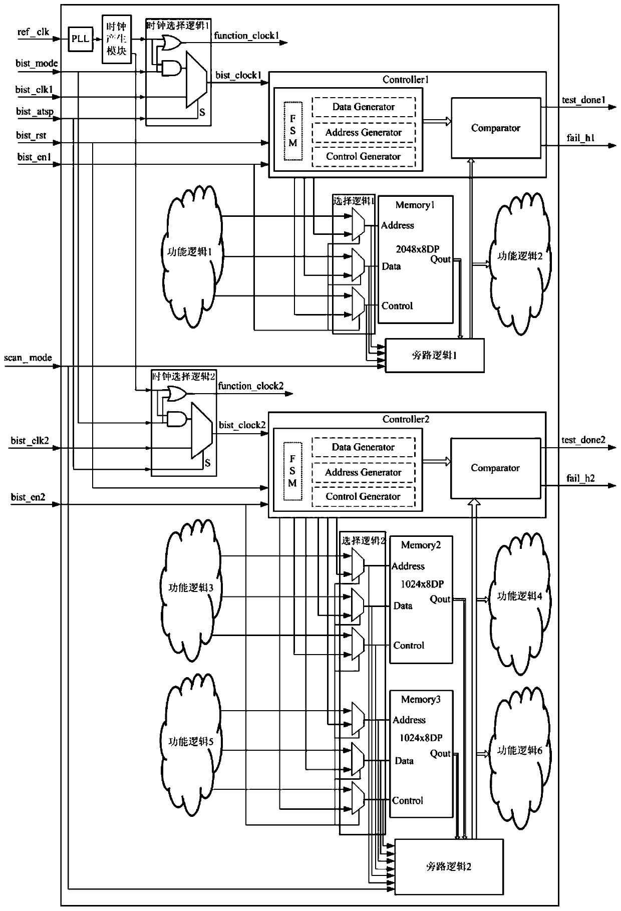
[0033] Take three memories Memory1, Memory2, and Memory3 on a single chip as an example, where Memory1 is a dual-port, the size is 2048 (that is, the address line width is 11 bits), the bit width is 8 bits, and the operating frequency is 120MHz. Both Memory2 and Memory3 are single ports, the size is 1024 (that is, the address line width is 10 bits), the bit width is 8 bits, and the working frequency is 60MHz. And in terms of layout, the distance between Memory2 and Memory3 is relatively close.

[0034] Using a batch tool, generate BIST libraries for the three memories. It is determined that Memory1 needs a controller Controller1, and Memory2 and Memory3 share a controller Controller2.

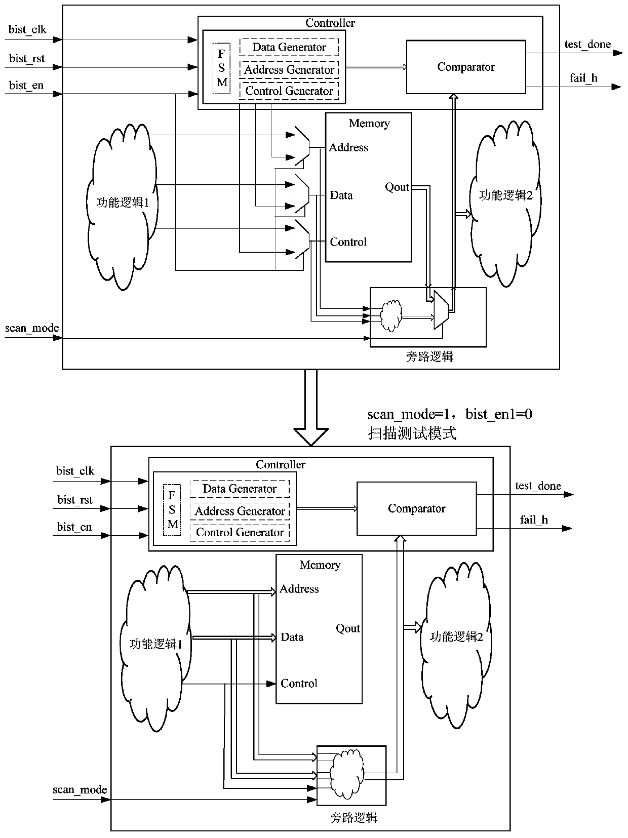
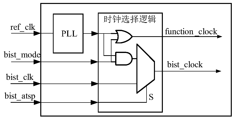
[0035] Add 2 memory test clock ports bist_clk1 and bist_clk2, memory test logic reset port bist_rst, 2 memory test enable ports bist_en1 and bist_en2, scan test mode port scan_mode, 2 memory test pass ports test_done1 and test_done2, 2 for a single chip Memory test fail ports fail_h1 and fail...


PUM


Abstract

The invention discloses a built-in self-test designing method of multiple embedded memories on single chip. In the method, reasonable memory built-in self-test scheme and structure are determined according to the working frequency, size, port type, number and layout of memories on a chip; in design, multiple memory built-in self-test logics are inserted, a test way of multiple combinations of serial and parallel tests is realized, the test time, test cost, test power consumption and area increase of test logics of the memories are optimized, the test efficiency is improved, and the layout wiring and timing closure in layout design are facilitated; a clock selection logic circuit is added to realize high-speed test and low-speed test; and moreover, with additional bypass logic of the memory, the loss of test coverage in a digital logic scanning test caused by the memory shadow logic can be eliminated, and the test coverage is increased.

Description

technical field [0001] The invention relates to a design method of Memory Built-In Self Test (MBIST) of multiple embedded memories on a single chip, especially the MBIST design when the working frequency of each memory differs greatly and the layout positions are far apart. The method belongs to the field of semiconductor digital integrated circuit design and testing, and is mainly applied to the MBIST design process of on-chip embedded memory of the semiconductor digital integrated circuit. Background technique [0002] With the development of integrated circuits, the integration level of chips has increased rapidly, and the proportion of embedded memory in the entire chip is increasing. The use of faster and larger on-chip memories is an inevitable development trend in the future. The method of testing memory based on functional vectors is not accepted by chip design manufacturers due to the constraints of test difficulty, test coverage and test efficiency. At present, th...

Claims


Application Information

Patent Timeline
Patent Type & Authority Patents(China)
IPC IPC(8): G11C29/16
CPCG11C29/16G11C2029/0401
Inventor 喻贤坤姜爽王莉彭斌樊旭孔瀛袁超
Owner BEIJING MXTRONICS CORP
Why Eureka
Try Eureka