Low-temperature polysilicon array substrate and manufacturing method thereof

A technology of low-temperature polysilicon and manufacturing methods, applied to semiconductor devices, electrical components, circuits, etc., can solve problems such as increased process complexity and uneven threshold voltage of polysilicon thin film transistors, and achieve the effect of increasing process complexity

Active Publication Date: 2021-01-26
BOE TECH GRP CO LTD
View PDF10 Cites 0 Cited by
  • Summary
  • Abstract
  • Description
  • Claims
  • Application Information

AI Technical Summary

Problems solved by technology

[0004] In view of the above-mentioned problems in the prior art, the purpose of the present invention is to provide a low-temperature polysilicon array substrate and its manufacturing method, which can solve the problem of uneven threshold voltage of polysilicon thin film transistors in the prior art without increasing the complexity of the process

Method used


Image

  • Low-temperature polysilicon array substrate and manufacturing method thereof
  • Low-temperature polysilicon array substrate and manufacturing method thereof
  • Low-temperature polysilicon array substrate and manufacturing method thereof

Examples


Embodiment 1

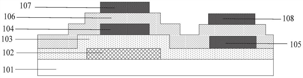
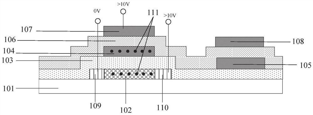
[0024] This embodiment provides a low-temperature polysilicon array substrate, figure 1 The structure of the low temperature polysilicon array substrate according to the embodiment of the present invention is shown.

[0025] Such as figure 1 As shown, the low-temperature polysilicon array substrate according to this embodiment includes: a substrate 101; an active layer 102 disposed on the substrate 101; a first gate insulating layer 103 disposed on the active layer 102, and the first insulating layer 103 covers The active layer 102 extends on the substrate 101; the first gate layer 104 formed on the first insulating layer 103, the first gate layer 104 is above the active layer 102, and also includes on the first insulating layer 103 The first capacitive electrode layer 105, the first capacitive electrode layer 105 is formed on the side of the substrate 101 away from the active layer 102; the second gate insulating layer 106 covers the first gate layer 104 and the first capaci...

Embodiment 2

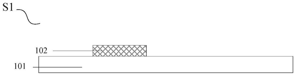
[0031] This embodiment provides a method for manufacturing a low-temperature polysilicon array substrate, which is used to manufacture the low-temperature polysilicon array substrate described in Embodiment 1. Figure 3 to Figure 8 A process flow chart of manufacturing a low-temperature polysilicon array substrate according to an embodiment of the present invention is shown.

[0032] Such as Figure 3 to Figure 8 As shown, the method for manufacturing a polysilicon array substrate according to this embodiment includes the following steps.

[0033] Such as image 3 As shown, first, in step S1, a transparent substrate such as glass that has been cleaned in advance is provided as the substrate 101, and a buffer layer including silicon oxide, silicon nitride, or a stack of the two can be formed on the substrate 101 to prevent the transparent substrate from The impurity of metal ions diffuses into the active layer and affects the working characteristics of TFT. Or a flexible subst...


PUM

PropertyMeasurementUnit
thicknessaaaaaaaaaa
thicknessaaaaaaaaaa
thicknessaaaaaaaaaa

Abstract

The present invention provides a low-temperature polysilicon array substrate structure, comprising: a substrate; an active layer on the substrate; a first gate insulating layer on the active layer; an insulating layer on the first gate A first gate layer above the active layer; a second gate insulating layer covering the first gate layer; between the second gate insulating layer A second gate layer on the top, the second gate layer is above the first gate layer. The present invention is beneficial to solve the problems of non-uniform display defect caused by non-uniform threshold voltage of polysilicon thin-film transistors in the prior art, and threshold voltage drift during process or use, without increasing process complexity.

Description

technical field [0001] The invention relates to the technical field of display devices, in particular to a low-temperature polysilicon array substrate and a manufacturing method thereof. Background technique [0002] The low-temperature polysilicon array substrate has the advantages of high mobility (up to hundreds of times that of amorphous silicon), the size of its thin film transistors can be made small, and the response speed is fast. It is a display panel that has become more and more popular in recent years. Array substrates are increasingly used in high-resolution, high-quality organic electroluminescent displays and liquid crystal display panels. However, the composition of low-temperature polysilicon array substrates is generally more complex, and the process is various, especially because the uniformity of polysilicon prepared by the current mainstream excimer laser crystallization method is difficult to maintain, and the uniformity of its threshold voltage is poor...

Claims


Application Information

Patent Timeline
Patent Type & Authority Patents(China)
IPC IPC(8): H01L27/12
CPCH01L27/1214H01L27/1248H01L27/1259
Inventor 刘政李小龙秦心宇
Owner BOE TECH GRP CO LTD
Why Eureka
Try Eureka