Display panel manufacturing method, display panel and display device

A display panel and manufacturing method technology, applied in semiconductor/solid-state device manufacturing, organic semiconductor devices, electrical components, etc., can solve problems such as easy cracks, packaging reliability test failure, difficult control of display panel cutting yield, etc., to achieve The effect of improving the cutting yield

Active Publication Date: 2017-06-20
BOE TECH GRP CO LTD +1
View PDF4 Cites 8 Cited by
  • Summary
  • Abstract
  • Description
  • Claims
  • Application Information

AI Technical Summary

Problems solved by technology

[0004] When the inventor applied the prior art, he found that if the prior art cut the display panel with a narrow frame according to the current cutting method, cracks would easily occur at the corners of the encapsulant, which would cause the package reliability test to fail, resulting in the cutting of the display panel. Yield is difficult to control

Method used


Image

  • Display panel manufacturing method, display panel and display device
  • Display panel manufacturing method, display panel and display device
  • Display panel manufacturing method, display panel and display device

Examples


Embodiment 1

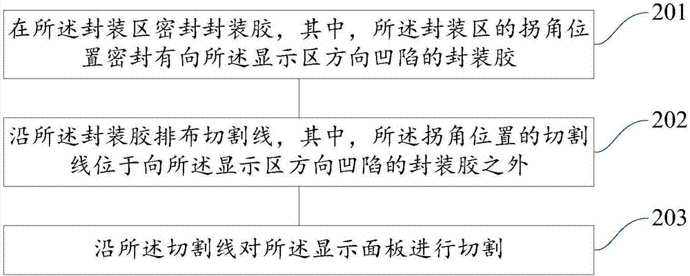
[0028] refer to figure 2 , which shows a flow chart of a method for manufacturing a display panel according to Embodiment 1 of the present invention, which may specifically include the following steps:

[0029] Step 201 , sealing the encapsulation area with an encapsulation glue, wherein the corners of the encapsulation area are sealed with an encapsulant recessed toward the display area.

[0030] In an embodiment of the present invention, the display motherboard includes at least one display panel, and each display panel has a display area and a packaging area surrounding the display area. Firstly, a silk screen with corners recessed inward is made, wherein the pattern of the screen corresponds to the size and position of each display panel in the display motherboard. Wherein, the display panel is an OLED panel, and the OLED panel includes an AMOLED (Active Matrix / Organic Light Emitting Diode, Active Matrix Organic Light Emitting Diode) panel

[0031] refer to image 3 As...

Embodiment 2

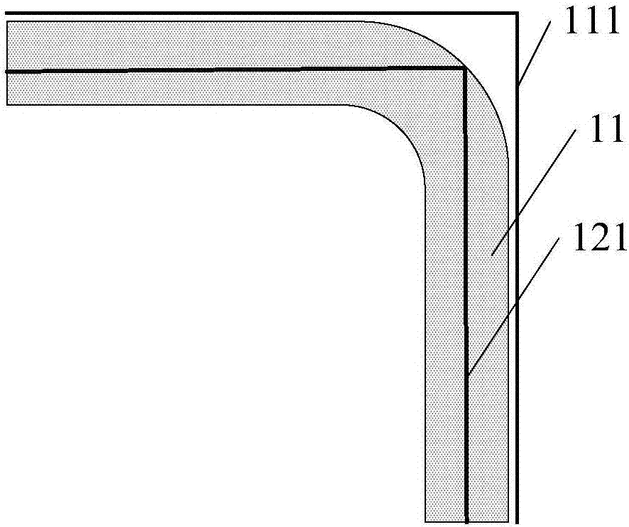
[0052] An embodiment of the present invention provides a display panel, which has a display area and an encapsulation area surrounding the display area, and an encapsulant recessed toward the display area is formed at a corner of the encapsulation area.

[0053] Specifically, the display motherboard includes at least one display panel, and each display panel has a display area and a packaging area surrounding the display area.

[0054] Firstly, a silk screen with corners recessed inward is made, wherein the pattern of the screen corresponds to the size and position of each display panel in the display motherboard.

[0055] Then, seal the encapsulation glue in the encapsulation area by screen printing according to the inwardly recessed screen corners. Since the inwardly recessed corners of the encapsulation area form a directional display area The encapsulant with concave direction. Wherein, the display panel is an OLED panel, and the packaging glue includes glass glue, which ...

Embodiment 3

[0063] A display device is provided in an embodiment of the present invention, and the display device includes the above-mentioned display panel.

[0064] The display panel has a display area and an encapsulation area surrounding the display area, and an encapsulant recessed toward the display area is formed at a corner of the encapsulation area.

[0065] Arranging cutting lines along the encapsulation, wherein the cutting lines at the corners are located outside the encapsulation recessed toward the display area; according to the arranged cutting lines, each display panel is cut along the cutting lines to obtain a separated Multiple display panels.

[0066] The display panel is an OLED panel, the height of the encapsulant is 4-10 μm, and the width of the non-depression in the encapsulant is greater than 300 μm.

[0067] In a preferred embodiment of the present invention, the width of the non-depression in the encapsulant is 300-700 μm.

[0068] The display device may be any...


PUM


Abstract

The embodiments of the invention provide a display panel manufacturing method, a display panel and a display device, and relate to the technical field of display. The display panel comprises a display area and a package area around the display area. The package area is sealed with package resin. The corners of the package area are sealed with package resin recessed towards the display area, and a cutting line is arranged along the package resin. The cutting line at the corners is disposed outside the package resin recessed towards the display area, and the display panel is cut along the cutting line. In order to get a narrow-bezel display panel, the package resin at the corners of the package area is designed in such a way that the package sin is recessed towards the display area, and thus, the cutting line at the corners is disposed outside the package resin. The problem that package reliability test fails as the package area can easily crack at the corners is eliminated, and the cutting yield of the display panel is increased.

Description

technical field [0001] The present invention relates to the field of display technology, in particular to a method for manufacturing a display panel, a display panel and a display device. Background technique [0002] With the continuous development of display technology, the frame width of the display panel is also becoming narrower, and the cutting difficulty of the display panel becomes more and more difficult due to the continuous narrowing of the frame frame of the display panel. [0003] refer to figure 1 , showing a partial cross-sectional view of an existing encapsulant, such as figure 1 As shown, the encapsulant 11 at the corner of the display panel is designed in a circular arc shape, the corner of the cutting line 111 is located outside the encapsulant 11, and the display panel is cut along the edge of the encapsulant 11. According to this cutting method, the The frame of the display panel is wider; such as figure 1 As shown, the corner of the cutting line 121 ...

Claims


Application Information

Patent Timeline
Patent Type & Authority Applications(China)
IPC IPC(8): H01L51/52H01L51/56
CPCH10K50/84H10K71/00H10K71/851H10K59/87H10K59/12
Inventor 李发顺白雪飞李伟
Owner BOE TECH GRP CO LTD
Why Eureka
Try Eureka