Circuit board structure and manufacturing method thereof

A technology of circuit structure and production method, which is applied in the direction of printed circuit manufacturing, printed circuit, printed circuit, etc., can solve the problems of limiting the layout of core layer circuits and reducing the flexibility of core layer wiring, and achieve the effect of large layout space

Active Publication Date: 2017-06-23
UNIMICRON TECH CORP
View PDF2 Cites 2 Cited by
  • Summary
  • Abstract
  • Description
  • Claims
  • Application Information

AI Technical Summary

Problems solved by technology

However, since the para-copper layer is directly formed on the core layer of the inner line layer, the line layout of the core layer is limited, thereby reducing the wiring flexibility of the core layer

Method used


Image

  • Circuit board structure and manufacturing method thereof
  • Circuit board structure and manufacturing method thereof
  • Circuit board structure and manufacturing method thereof

Examples


Embodiment Construction

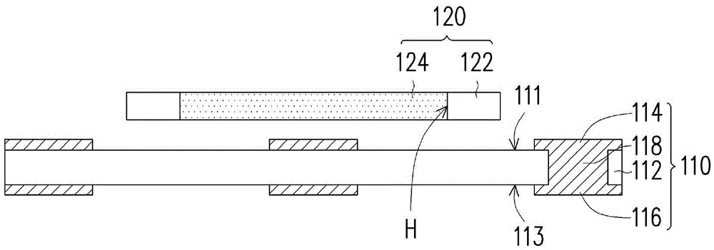
[0058] Figure 1A(a) to Figure 1J It is a schematic cross-sectional view of a manufacturing method of a circuit board structure according to an embodiment of the present invention. Please refer to FIG. 1A (a) first, regarding the manufacturing method of the circuit board structure of the present embodiment, at first, an inner layer circuit structure 110 is provided, wherein the inner layer circuit structure 110 includes a core with an upper surface 111 and a lower surface 113 opposite to each other layer 112 , a first patterned circuit layer 114 disposed on the upper surface 111 , and a second patterned circuit layer 116 disposed on the lower surface 113 . As shown in FIG. 1A( a ), the first patterned circuit layer 114 and the second patterned circuit layer 116 can be electrically connected through at least one conductive via 118 penetrating through the core layer 112 .

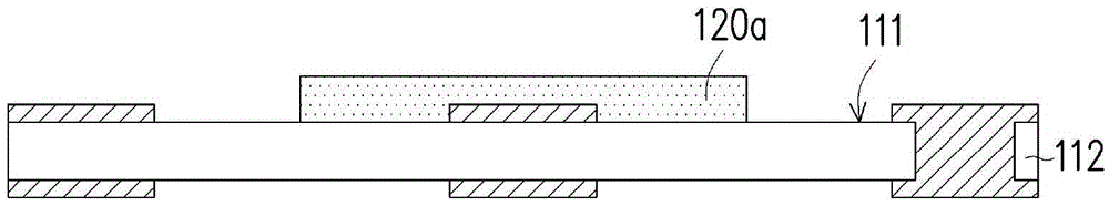
[0059] Next, please also refer to the Figure 1A(a) and 1B(a) , forming an insulating material layer 12...


PUM


Abstract

The invention provides a circuit board structure and a manufacturing method thereof. The method includes following steps: providing an internal layer line structure, wherein the internal layer line structure comprises a core layer including an upper surface and a lower surface opposite to each other, a first patterning line layer configured on the upper surface, and a second patterning line layer configured on the lower surface; forming an insulating material layer on a part of the first patterning line layer; forming a laser barrier layer on at least a part of the insulating material layer; attaching a release layer on the laser barrier layer; performing a lamination process, and respectively pressing a first lamination line structure and a second lamination line structure on the first patterning line layer and the second patterning line layer; and performing a laser ablation process, and forming a groove which at least exposes a part of the upper surface of the core layer. According to the formed circuit board structure, the wiring flexibility is good, and a larger layout space can be provided.

Description

technical field [0001] The invention relates to a circuit board structure and a manufacturing method thereof, in particular to a circuit board structure with grooves and a manufacturing method thereof. Background technique [0002] Generally speaking, to make a circuit board structure with grooves, it is usually necessary to make a para-position copper layer on the core layer of the inner circuit layer. The purpose is to form the grooves by subsequent laser ablation of the circuit structure. During the process, the alignment copper layer can be regarded as a laser blocking layer to avoid excessive ablation of the circuit structure, and can also be regarded as a laser alignment pattern, which is beneficial to the laser ablation process. However, since the para-copper layer is directly formed on the core layer of the inner circuit layer, the circuit layout of the core layer is limited, thereby reducing the wiring flexibility of the core layer. Contents of the invention [0...

Claims


Application Information

Patent Timeline
Patent Type & Authority Applications(China)
IPC IPC(8): H05K3/00
CPCH05K3/0011H05K2201/09036H05K2203/107
Inventor 张宏麟吴明豪张训効余丞博张启民
Owner UNIMICRON TECH CORP
Why Eureka
Try Eureka