High-precision LED circuit board forming process without process edge

A technology of LED circuit board and molding process, applied in the directions of printed circuit, printed circuit manufacturing, electrical components, etc., can solve the problems of rough punching edge, crushed metal surface, large shape tolerance, etc., to improve processing precision, guarantee Product quality, the effect of reducing external dimension tolerances

Active Publication Date: 2017-06-27
VICTORY GIANT TECH HUIZHOU CO LTD
View PDF13 Cites 22 Cited by
  • Summary
  • Abstract
  • Description
  • Claims
  • Application Information

AI Technical Summary

Problems solved by technology

The first molding method relies on the positioning holes set in the circuit board. When the gong board is formed, the force of the gong knife has a greater impact on the board, resulting in a large shape tolerance, and the shape tolerance is greater than 0.1mm; the second type The forming method relies on stamping model processing, which has quality risks such as rough punching edges and crushed metal surfaces; the third forming method relies on

Method used


Image

  • High-precision LED circuit board forming process without process edge
  • High-precision LED circuit board forming process without process edge

Examples


Embodiment Construction

[0014] In order to facilitate those skilled in the art to understand the present invention, the present invention will be further described in detail below in conjunction with specific embodiments and accompanying drawings.

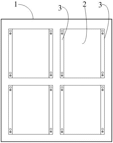
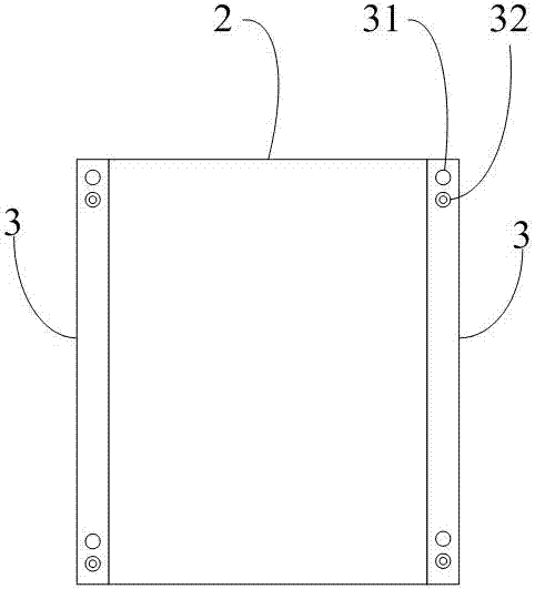
[0015] First, in the PNL board 1 (production board), carry out the board design for the product shape of each LED circuit board 2, and design the auxiliary process side 3 on the shape side of each LED circuit board 2 in the PNL board 1, such as figure 1 As shown, the LED circuit board 2 is square, and an auxiliary process side 3 is designed on both sides of the LED circuit board 2 . And set positioning holes 31 and optical points 32 on the auxiliary process side 3, such as figure 2 As shown, four positioning holes 31 and four optical points 32 are designed for each LED circuit board, and the positioning holes 31 and optical points 32 are arranged in pairs at the two ends of the auxiliary process side 3 of the LED circuit board 2, and the positioning hole...


PUM


Abstract

The present invention provides a high-precision LED circuit board forming process without a process edge. The process comprises the steps: performing routing design aiming at the shape of the product of a LED circuit board, designing an auxiliary process edge at the shape edge of each LED circuit board in a PNL board, and arranging location holes and optical points on the auxiliary process edge; according to the routing design, employing the location holes on the auxiliary process edge for location, performing rough routing processing of each LED circuit board, and performing routing of the PNL board to a SET board keeping the auxiliary process; and employing the optical points on the auxiliary process edge for location, employing a CCD optical routing machine to complete the fine routing of the LED circuit board, and removing the auxiliary process edge of each LED circuit board in the SET board.

Description

technical field [0001] The invention relates to the field of circuit board manufacturing, in particular to a high-precision LED circuit board forming process without process edges. Background technique [0002] In some electronic products, due to their small size and compact internal space, it is required to have no process edge on the circuit board when making and forming the circuit board, so as to reduce the space occupied by the circuit board as much as possible, and without the process edge for auxiliary positioning, it is necessary to use Special positioning forming method. At present, the forming method of the circuit board without process edge is forming the positioning hole in the board, die punching, and the edge of the board is formed by the pin. The first molding method relies on the positioning holes set in the circuit board. When the gong board is formed, the force of the gong knife has a greater impact on the board, resulting in a large shape tolerance, and th...

Claims


Application Information

Patent Timeline
IPC IPC(8): H05K3/00
CPCH05K3/0044
Inventor 杨晓彬胡汉民宋强郭建峰
Owner VICTORY GIANT TECH HUIZHOU CO LTD
Why Eureka
Try Eureka