

Touch display substrate, touch display device and touch display method
A technology for touch display substrates and touch display devices, applied in optics, instruments, electrical digital data processing, etc., can solve problems such as pulling and affecting the stability of touch performance, and achieve the effect of eliminating pulling effects and ensuring stability
- Summary
- Abstract
- Description
- Claims
- Application Information
AI Technical Summary
Problems solved by technology
Method used
Image

Examples
Embodiment Construction
[0031] In order to further illustrate the touch display substrate, touch display device and touch display method provided by the embodiments of the present invention, a detailed description will be given below in conjunction with the accompanying drawings.
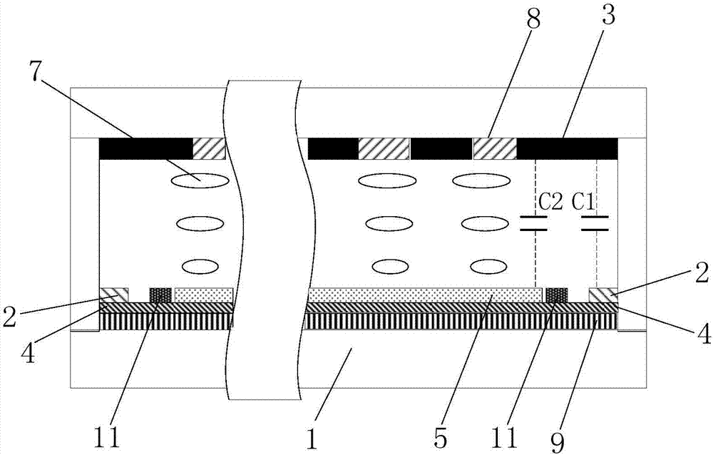
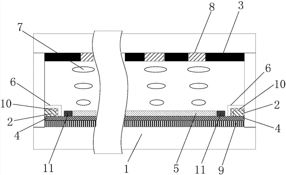
[0032] see figure 1 , as described in the background art, in the prior art, since the edge line 2 located in the non-touch area of the touch display substrate is opposite to the black matrix 3 on the opposite substrate, when the touch display device works in the touch period, The first parasitic capacitance C1 will be generated between the edge line 2 and the black matrix 3, and the second parasitic capacitance C2 will be generated between the black matrix 3 and the transparent conductive electrode 5 at the same time, so that the first parasitic capacitance C1 and the second parasitic capacitance C2 A coupling effect easily occurs between them, causing the electrical signal on the transparent conductive electrode 5 to be...
PUM
 Abstract
Description
Claims
Application Information