A silicon-based display based on fusion scanning strategy

A display, silicon-based technology, used in static indicators, instruments, etc., can solve problems such as high data bandwidth, reduce area requirements, reduce circuit scanning speed requirements, and improve conversion accuracy and conversion speed.

Active Publication Date: 2020-07-31
南京昀光科技有限公司
View PDF5 Cites 0 Cited by
  • Summary
  • Abstract
  • Description
  • Claims
  • Application Information

AI Technical Summary

Problems solved by technology

However, under the conditions of high resolution and high refresh rate, the digital scanning strategy requires extremely high data bandwidth, which poses higher challenges to system performance

Method used


Image

  • A silicon-based display based on fusion scanning strategy
  • A silicon-based display based on fusion scanning strategy
  • A silicon-based display based on fusion scanning strategy

Examples


Embodiment 1

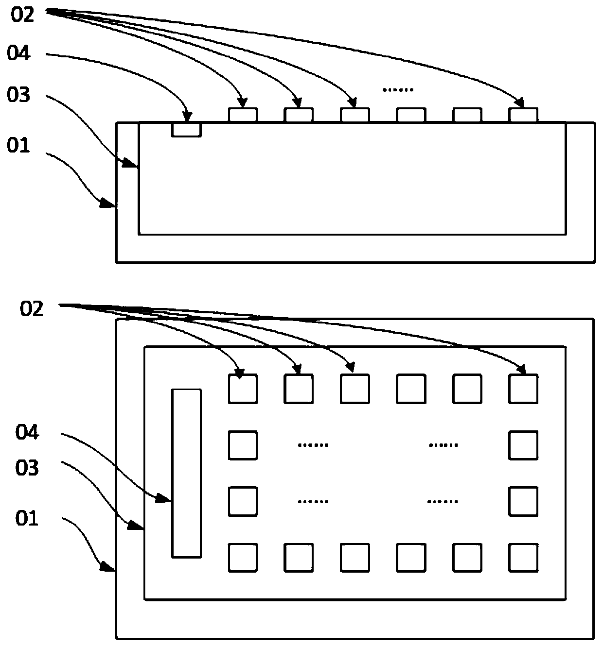
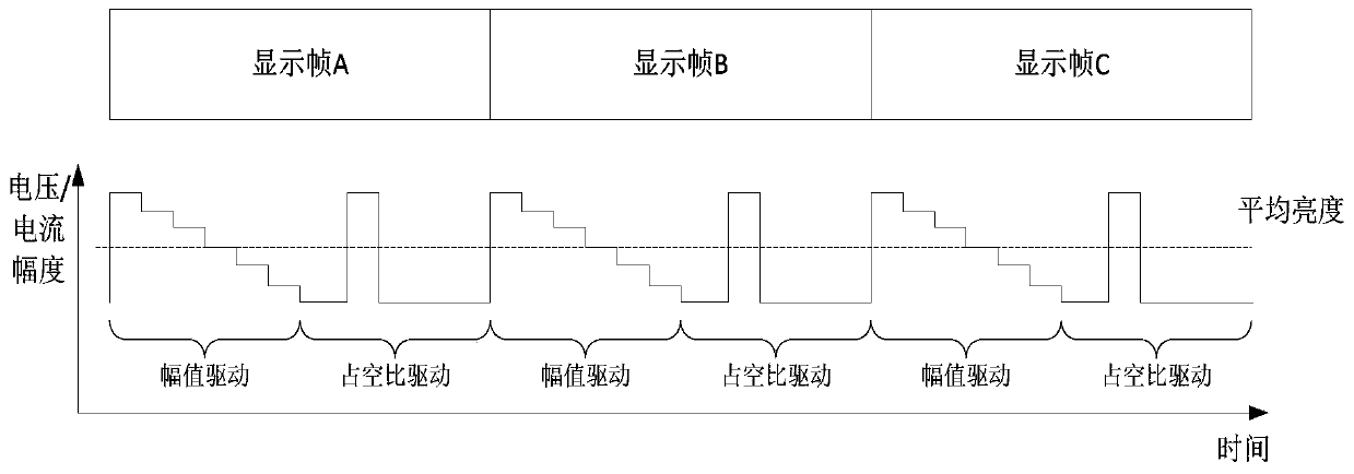
[0041] figure 1 The basic structure of a silicon-based microdisplay adopted in the present invention is illustrated, the upper part is a side view, and the lower part is a top view, which at least includes a semiconductor silicon substrate 01 and a pixel 02 on the surface of the silicon substrate and a driving circuit 03 contained in the silicon substrate and Interface 04, the drive circuit 03 at least includes a metal-oxide semiconductor field effect transistor and at least two metal layers; the brightness of the pixel 02 in a specific display frame is determined by the output current or voltage of the pixel in the display frame The amplitude of the pixel and the time duty cycle of the output current or voltage of the pixel in the display frame are jointly determined; the display frame includes the pixel grayscale information in a specific display area through the interface 04 through the drive circuit 03 is the process of transmitting to the pixel 02; the specific display fr...

Embodiment 2

[0045] This embodiment is basically the same as Embodiment 1, especially in that:

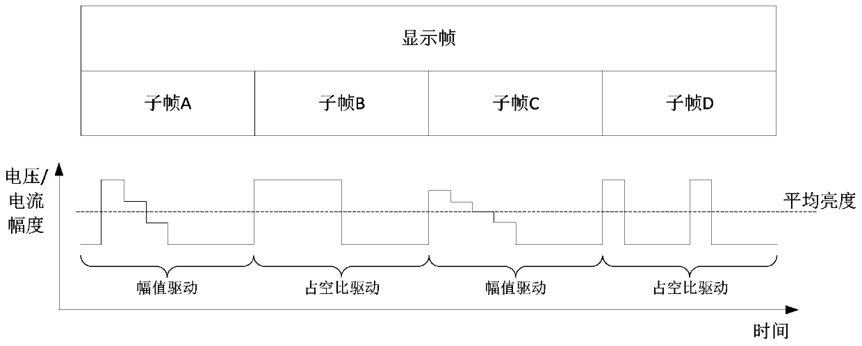
[0046] In any subframe, the brightness of a pixel is jointly determined by the magnitude of the output current or voltage of the pixel in the subframe and the time duty cycle of the output current or voltage of the pixel in the subframe. Brightness The brightness in the specific display frame is equivalent to the average brightness of the pixel in all sub-frames in the specific display frame.

[0047] The process is a sequential transmission process or a random transmission process. The sequential transmission means that the grayscale information is transmitted point by point in the order from row to column or from column to row. The random transmission means that the grayscale information Information is transmitted randomly in random row or random column order.

[0048] The specific subset is one or more bit planes of pixel grayscale data in the specific display area, the bit plane is a data ...

Embodiment 3

[0052] This embodiment is basically the same as Embodiment 1, especially in that:

[0053] The subframe can be further divided into several repeated frames, the repeated frames include the process of repeatedly transmitting the same grayscale information to the pixel 02, and the grayscale information transmitted by each repeated frame is consistent with the The information required to be transmitted in a subframe is exactly the same, the sum of the time lengths of all repeated frames in each subframe is equal to the total time length of the subframe, and the time order of the repeated frames belonging to different subframes is in order within a display frame or randomly arranged. Figure 5 An example of displaying subframe repeating frame driving waveforms for silicon-based microdisplays, including two sets of repeating frames A1 / A2 and B1 / B2, where A1 and A2 are repeating frames of subframe A, and B1 and B2 are repeating frames of subframe A. For the repeated frames of frame...


PUM


Abstract

The invention discloses a silicon-based display device based on a fused scanning strategy, wherein the display device relates to the field of microelectronic panel displaying technology. Brightness of a pixel in a specific display frame is determined by amplitude of output current or voltage of the pixel in the display frame and time duty ratio of the output current or voltage of the pixel in the display frame. A specific display frame is divided into a plurality of subframes. The subframe comprises a process of transmitting a specific subset of pixel gray scale information in a specific display area to the pixel through an interface by means of a driving circuit. The silicon-based display device reduces precision requirement of a digital-to-analog converter and a pixel circuit and improves conversion precision and conversion speed of the digital-to-analog converter. The silicon-based display device further has advantages of breaking restriction of resolution and refresh rate of a silicon-based micro display device by limitation of a scanning driving mode, reducing area requirement of the digital-to-analog converter and a pixel unit circuit, reducing area and complexity of the circuit, further improving pixel density, and improving gray scale number and contrast of the pixel.

Description

technical field [0001] The invention relates to the technical fields of microelectronics and flat panel display, in particular to a silicon-based microdisplay based on a fusion scanning strategy. Background technique [0002] A silicon-based microdisplay is a microdisplay based on a silicon semiconductor integrated circuit, and the driver circuit of the display is integrated in the silicon substrate. According to different display principles, silicon-based microdisplays can be divided into silicon-based organic light-emitting microdisplays, silicon-based light-emitting diode microdisplays, silicon-based liquid crystal microdisplays, and silicon-based micromechanical microdisplays. The pixels of silicon-based microdisplays are very small, and it produces a large-screen display effect through an optical system, which can be applied to military, industrial, medical and consumer electronics. At present, silicon-based microdisplays are developing toward higher resolution, higher...

Claims


Application Information

Patent Timeline
Patent Type & Authority Patents(China)
IPC IPC(8): G09G3/20
CPCG09G3/20
Inventor 季渊余云森褚勇男穆廷洲沈伟星
Owner 南京昀光科技有限公司
Why Eureka
Try Eureka