

Array substrate and manufacturing method thereof, and organic light emitting display
A technology for light-emitting displays and organic light-emitting devices, which is applied in semiconductor/solid-state device manufacturing, semiconductor devices, electric solid-state devices, etc., and can solve the problems of easy-off positions and offsets of support columns, so as to avoid falling-off or position shifting and lifting The effect of impact resistance
- Summary
- Abstract
- Description
- Claims
- Application Information
AI Technical Summary
Problems solved by technology
Method used
Image

Examples
Embodiment 1
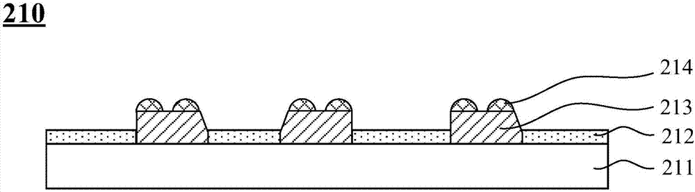
[0035] Please refer to image 3 , which is a cross-sectional view of the array substrate according to Embodiment 1 of the present invention. Such as image 3 As shown, the array substrate 210 includes: a substrate 211, an organic light emitting device 212 formed on the substrate 211, a pixel definition layer 213 disposed between adjacent organic light emitting devices 212, and a pixel definition layer 213 formed on the The support column 214 on the pixel definition layer 213, the longitudinal section (section perpendicular to the surface of the substrate 211) of the support column 214 is an arc surface.
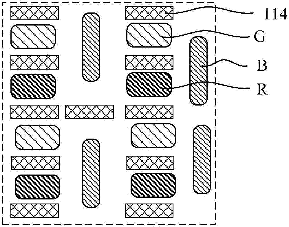
[0036] Specifically, please refer to Figure 3 to Figure 5 , the organic light emitting devices 212 (including the red sub-pixel R, the green sub-pixel G and the blue sub-pixel B) of the array substrate 210 are all located in the pixel opening area, the support pillars 214 are located outside the pixel opening area, and the support The column 214 is a rectangular ring stru...
Embodiment 2
[0044] Please refer to Figure 7 and Figure 8 , which is a schematic structural diagram of the array substrate according to Embodiment 2 of the present invention, as shown in Figure 7 and Figure 8 As shown, the array substrate 210 includes: a substrate 211, an organic light emitting device 212 formed on the substrate 211, a pixel definition layer 213 disposed between adjacent organic light emitting devices 212, and a pixel definition layer 213 formed on the The supporting pillars 214 (SPC layer) on the pixel definition layer 213, the longitudinal sections of the supporting pillars 214 (the cross section perpendicular to the surface of the substrate 211) are arc-shaped.
[0045] Specifically, such as Figure 7 and Figure 8 As shown, the organic light emitting devices 212 (including the red sub-pixel R, the green sub-pixel G and the blue sub-pixel B) of the array substrate 210 are all located in the opening area, the support columns 214 are located in the light-shielding...
Embodiment 3
[0049] Please refer to Figure 9 and Figure 10 , which is a schematic structural diagram of the array substrate according to Embodiment 3 of the present invention, as shown in Figure 9 and Figure 10 As shown, the array substrate 210 includes: a substrate 211, an organic light emitting device 212 formed on the substrate 211, a pixel definition layer 213 disposed between adjacent organic light emitting devices 212, and a pixel definition layer 213 formed on the The support pillars 214 (SPC layer) on the pixel definition layer 213, the longitudinal sections (sections perpendicular to the surface of the substrate) of the support pillars 214 are arc-shaped.
[0050] Specifically, such as Figure 9 and Figure 10 As shown, the organic light emitting devices 212 (including the red sub-pixel R, the green sub-pixel G and the blue sub-pixel B) of the array substrate 210 are all located in the opening area, the support columns 214 are located in the light-shielding area, and the s...
PUM
 Abstract
Description
Claims
Application Information