Touch control display panel and touch control display device

A technology for touch display panels and touch electrodes, which is applied in the fields of instruments, computing, and electrical digital data processing, etc., and can solve problems such as large contact area of ​​two inorganic layers, serious stress accumulation and stress transmission, and fracture of inorganic layers

Active Publication Date: 2017-07-04
SHANGHAI TIANMA MICRO ELECTRONICS CO LTD
View PDF3 Cites 28 Cited by
  • Summary
  • Abstract
  • Description
  • Claims
  • Application Information

AI Technical Summary

Problems solved by technology

Since the insulating layer generally directly covers the metal layer by evaporation, the contact area between the two inorganic layers is relatively large, and the stress accumulation and stress transmission at the contact position between the insulating layer and the thin-film packaging layer are serious, and it is easy to make the insulating layer or thin film The outermost inorganic layer of the encapsulation layer away from the array substrate is broken, and once one of the inorganic layers is broken, the other inorganic layer will be broken

Method used


Image

  • Touch control display panel and touch control display device
  • Touch control display panel and touch control display device
  • Touch control display panel and touch control display device

Examples


Embodiment Construction

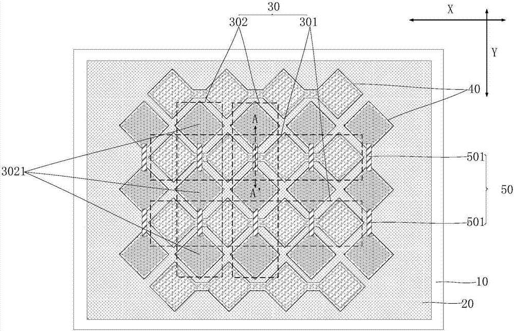
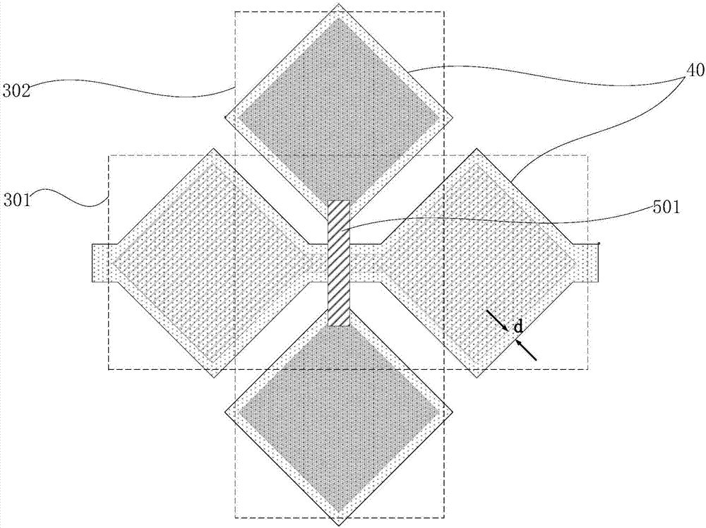
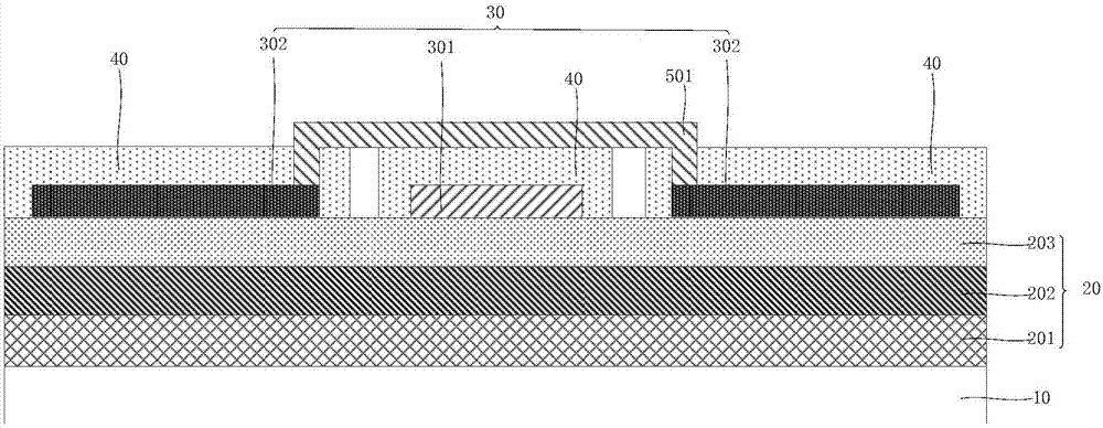
[0028] The present invention will be further described in detail below in conjunction with the accompanying drawings and embodiments. It should be understood that the specific embodiments described here are only used to explain the present invention, but not to limit the present invention. In addition, it should be noted that, for the convenience of description, only some structures related to the present invention are shown in the drawings but not all structures. Throughout this specification, the same or similar reference numerals represent the same or similar structures, elements or processes. It should be noted that, in the case of no conflict, the embodiments in the present application and the features in the embodiments can be combined with each other.

[0029] An embodiment of the present invention provides a touch display panel, including an organic light emitting element array substrate; a thin film encapsulation layer covering the organic light emitting element arra...


PUM


Abstract

The invention discloses a touch control display panel and a touch control display device. The touch control display panel comprises an organic light-emitting device array substrate; a film encapsulated layer which covers the organic light-emitting device array substrate; the film encapsulated layer comprises at least one inorganic layer and at least one organic layer; a patterning first conducting layer, a patterning insulating layer covering the patterning first conducting layer and a patterning second conducting layer are successively arranged on the outermost surface, away from the array substrate, of the film encapsulated layer; the patterning insulating layer and the patterning first conducting layer have the same patterns; and the material of the patterning insulating layer is inorganic material; the patterning first conducting layer and the patterning second conducting layer are insulated by the patterning insulating layer. By means of the technical scheme of the invention, the contact area of the pattering insulating layer and the film encapsulated layer is reduced, the stress accumulation and stress transmission between the patterning insulating layer and the film encapsulated layer are weakened and the risk of crack in the patterning insulating layer and the film encapsulated layer is reduced, which is good for flexible display.

Description

technical field [0001] The embodiments of the present invention relate to the field of touch technology, and in particular, to a touch display panel and a touch display device. Background technique [0002] A touch panel is an input device that senses a touch position of a user's finger or a tool, and a touch display panel is a device that integrates a touch function and a display function. At present, the touch display panel generally includes a thin-film encapsulation layer arranged on an array substrate to block external water and oxygen. The thin-film encapsulation layer generally includes stacked multi-layer organic layers and inorganic layers. Metal layers such as a touch electrode layer, a bridge layer, or a touch wiring layer may be disposed on the thin film encapsulation layer, and an insulating layer needs to be disposed between each metal layer to achieve mutual electrical insulation. [0003] The insulating layer is generally made of inorganic materials. When th...

Claims


Application Information

Patent Timeline
Patent Type & Authority Applications(China)
IPC IPC(8): G06F3/041G06F3/044
CPCG06F3/0412G06F3/044
Inventor 刘雪宁柳晨王丽花
Owner SHANGHAI TIANMA MICRO ELECTRONICS CO LTD
Why Eureka
Try Eureka