Phase change memory device having a reduced contact area and method for manufacturing the same

Inactive Publication Date: 2010-07-01
SK HYNIX INC
View PDF19 Cites 66 Cited by
  • Summary
  • Abstract
  • Description
  • Claims
  • Application Information

AI Technical Summary

Benefits of technology

[0009]A phase change memory device capable of reducing a contact area of a bottom electrode

Problems solved by technology

Unfortunately, with the ever continuous trend of increasingly concentrating the integration of the semiconductor memory devices, the critical dimensions needed to be achieved to form highly resolved patterns and holes are soon thought to be beyond the

Method used


Image

  • Phase change memory device having a reduced contact area and method for manufacturing the same
  • Phase change memory device having a reduced contact area and method for manufacturing the same
  • Phase change memory device having a reduced contact area and method for manufacturing the same

Examples


Embodiment Construction

.”

BRIEF DESCRIPTION OF THE DRAWINGS

[0015]The above and other aspects, features and other advantages of the subject matter of the present disclosure will be more clearly understood from the following detailed description taken in conjunction with the accompanying drawings, in which:

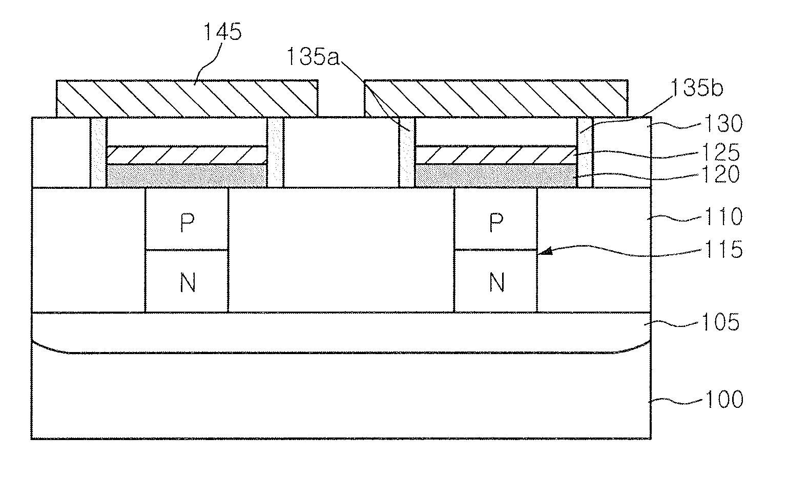
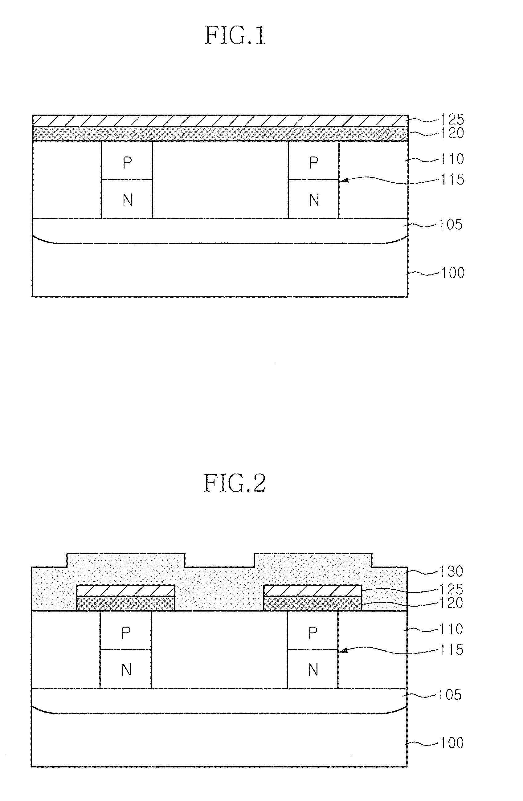
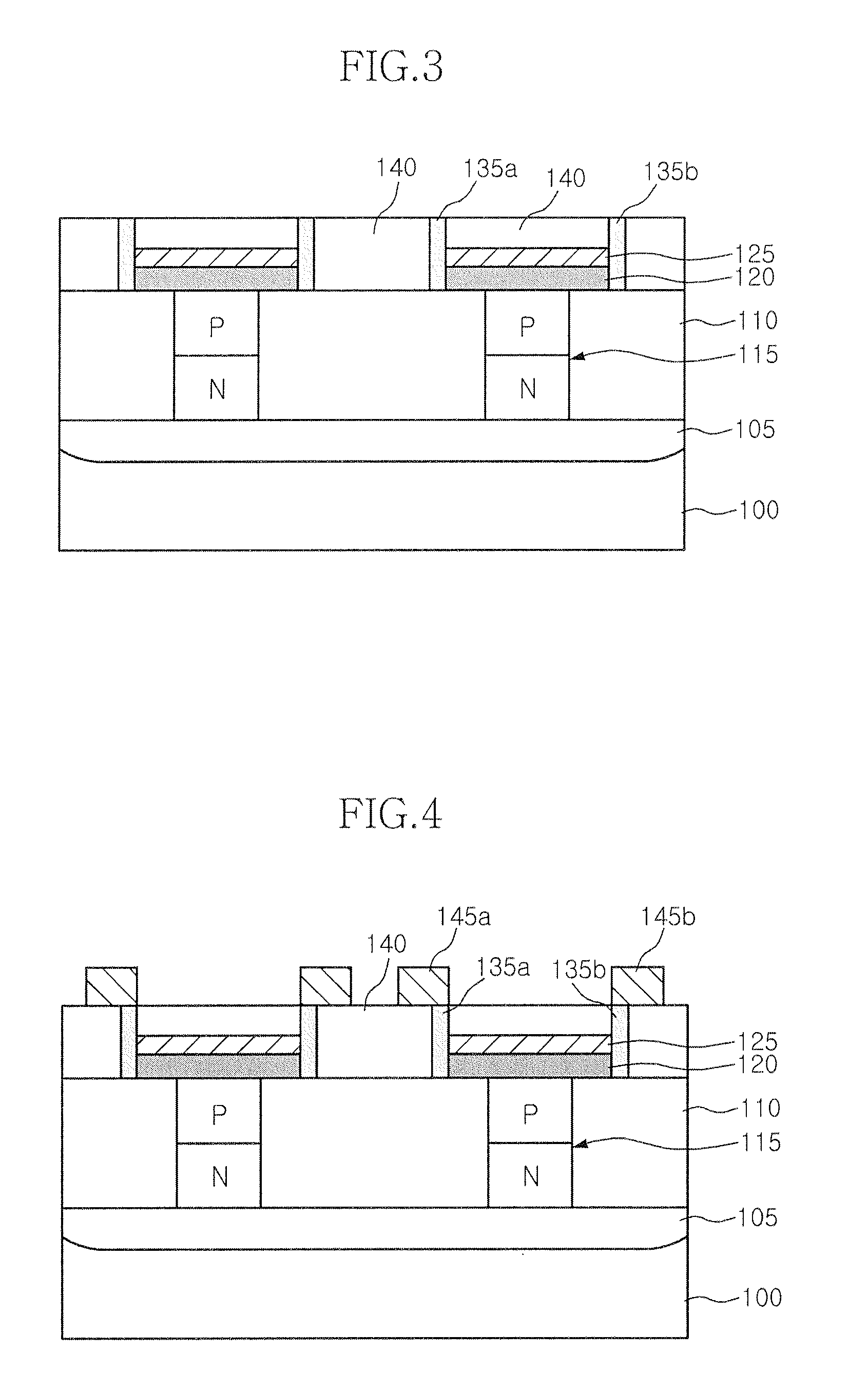
[0016]FIGS. 1 to 4 are cross-sectional views illustrating an example of a method for manufacturing a phase change memory device according to one embodiment;

[0017]FIG. 5 is a cross-sectional view illustrating an example of an example of a phase change memory device according to another embodiment;

[0018]FIG. 6 is an equivalent circuit of the phase change memory device according to one embodiment;

[0019]FIGS. 7 to 9 are cross-sectional views illustrating an example of a method for manufacturing a phase change memory device according to another embodiment;

[0020]FIG. 10 is a top view illustrating an upper electrode and a phase change pattern in the phase change memory device according to another embodiment; and

[...


PUM


Abstract

A phase change memory device having a reduced contact area and a method for manufacturing the same is presented. The phase change random access memory device includes a bottom electrode contact pattern layer, and at least one phase change pattern layer formed on a sidewall of the bottom electrode contact pattern layer. The contact areas are minimized by being between the narrow width of the bottom electrode contact pattern layer, i.e., at the sidewall, and the phase change pattern layers. As a result the minimized contact area is proportional to the thickness of the bottom electrode contact pattern layer.

Description

CROSS-REFERENCES TO RELATED APPLICATION[0001]The present application claims priority under 35 U.S.C. 119(a) to Korean application number 10-2008-0134269, filed on Dec. 26 2008, in the Korean Patent Office, which is incorporated by reference in its entirety as if set forth in full.BACKGROUND OF THE INVENTION[0002]1. Technical Field[0003]The embodiments described herein relate to a phase change memory device and a method for manufacturing the same and, more particularly, to a phase change memory device having a reduced contact area between the phase change layer and a bottom electrode contact and a method for manufacturing the same.[0004]2. Related Art[0005]With the rapid development of intellectual technologies, next generation memory devices having high-speed and mass storage characteristics are needed in the use of portable information telecommunication apparatuses and systems which process massive amounts of information by wireless communication schemes. Next generation memory dev...

Claims


Application Information

Patent Timeline
IPC IPC(8): H01L47/00H01L21/00
CPCH01L27/2409H01L45/06H01L45/124H01L45/144H01L45/1691H10B63/20H10N70/231H10N70/8265H10N70/8828H10N70/068H10N70/8825
Inventor SON, MIN SEOK
Owner SK HYNIX INC
Why Eureka
Try Eureka