Manufacturing method and structure for improving the characteristics of phase change memory

a manufacturing method and memory technology, applied in the direction of bulk negative resistance effect devices, electrical equipment, semiconductor devices, etc., can solve the problems of inconvenient pvd, phase change material cannot be deposited using physical vapor deposition (pvd) process, and material is not suitable for bending, so as to improve the characteristics of phase change memory, reduce contact area, and stable component characteristics

a manufacturing method and memory technology, applied in the direction of bulk negative resistance effect devices, electrical equipment, semiconductor devices, etc., can solve the problems of inconvenient pvd, phase change material cannot be deposited using physical vapor deposition (pvd) process, and material is not suitable for bending, so as to improve the characteristics of phase change memory, reduce contact area, and stable component characteristics

US20070040159A1Inactive Publication Date: 2007-02-22IND TECH RES INST

Image

  • Manufacturing method and structure for improving the characteristics of phase change memory
  • Manufacturing method and structure for improving the characteristics of phase change memory
  • Manufacturing method and structure for improving the characteristics of phase change memory

Examples


Embodiment Construction

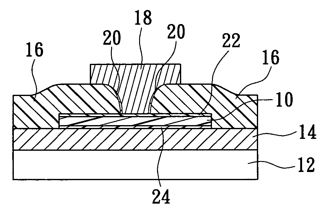
[0024] The present invention provides a simple manufacturing method for improving the characteristics of phase change memory. The method maintains a small contact area to reduce power consumption.

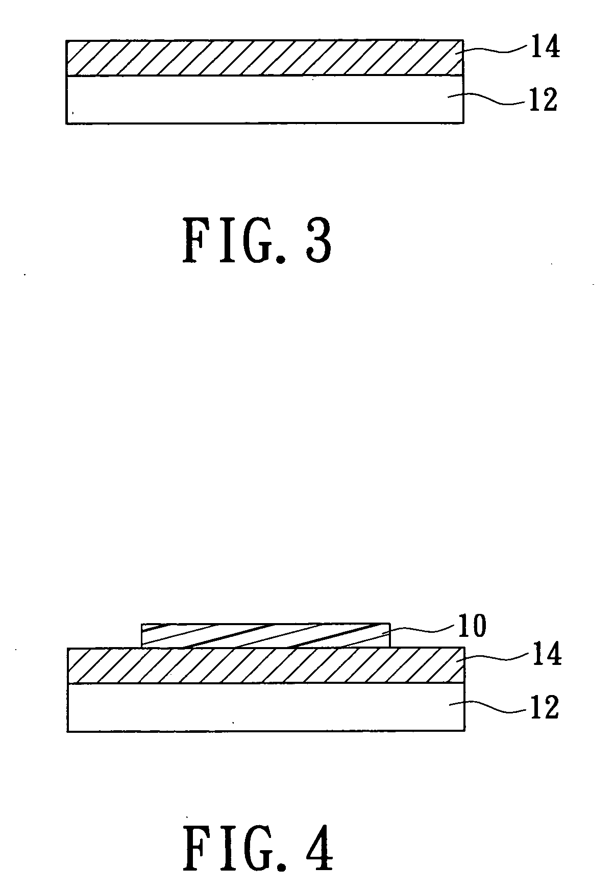
[0025] Please refer to FIG. 3, which is a process schematic depiction of the bottom electrode pattern in accordance with an embodiment of the present invention. A bottom electrode pattern 14 is formed on a substrate 12. The substrate 12 could be connected to CMOS, BJT or other driving devices.

[0026]FIG. 4 shows a schematic depiction of a process of the phase change layer pattern in accordance with an embodiment of the present invention. A layer of phase change material pattern 10 is formed on said bottom electrode pattern 14. In another embodiment at least one adhesive layer, at least one heating layer, or at least one etching stop layer is added on any side of the phase change material pattern 10 such that the etching is opened, the metal becomes adhesive, or heating efficiency is increa...


PUM


Abstract

A manufacturing method and structure for better phase change memory characteristics by improving the interface and the hole-filling properties. The present invention can reduce the power consumption needed to operate and is easy to fabricate.

Description

BACKGROUND OF THE INVENTION [0001] 1. Field of the Invention [0002] The present invention relates to a manufacturing method and structure for improving the characteristics of phase change memory. [0003] 2. Description of Related Art [0004] Energy Conversion Devices Inc. proposed ovonic unified memory (OUM) theory in the 1960s. Energy Conversion Devices Inc. discovered optic properties and a conductance ratio difference in phase change memory between its generally amorphous and generally crystalline states. Because Phase change materials have the characteristic of being able to switch between two phases rapidly it has two functions—firstly, it is able to act as a switch and secondly, it can act as a memory. Phase change memory uses chalcogenides (a kind of conductive glass) as the core material for phase change memory and needs to be connected to an electrode. Phase change memory can switch between the amorphous and crystalline states using different current pulses. The amorphous and...

Claims


Application Information

Patent Timeline
22 Feb 2007
Publication
US20070040159A1
IPC
H01L29/04
CPC
H01L45/06; H01L45/1233; H01L45/126; H01L45/16; H10N70/8413; H10N70/231; H10N70/011; H10N70/826
Inventors
WANG, WEN-HAN