Heat treatment device and wafer treatment method thereof

A technology for heat treatment equipment and wafers, used in electrical components, semiconductor/solid-state device manufacturing, circuits, etc., to solve the problems of large wafer surface leakage current and poor wafer surface state, to improve the surface state and ensure safety. , The effect of improving electrical properties and stability

Inactive Publication Date: 2017-07-07
WUXI CHINA RESOURCES HUAJING MICROELECTRONICS
View PDF5 Cites 3 Cited by
  • Summary
  • Abstract
  • Description
  • Claims
  • Application Information

AI Technical Summary

Problems solved by technology

[0005] Embodiments of the present invention provide a heat treatment device and a method for processing wafers there

Method used


Image

  • Heat treatment device and wafer treatment method thereof
  • Heat treatment device and wafer treatment method thereof
  • Heat treatment device and wafer treatment method thereof

Examples


Embodiment Construction

[0032] In order to make the purpose, technical solutions and advantages of the present invention clearer, the technical solutions of the present invention will be clearly and completely described through implementation with reference to the accompanying drawings in the embodiments of the present invention. Obviously, the described embodiments are the embodiment of the present invention. Some, but not all, embodiments. Based on the embodiments of the present invention, all other embodiments obtained by persons of ordinary skill in the art without making creative efforts belong to the protection scope of the present invention.

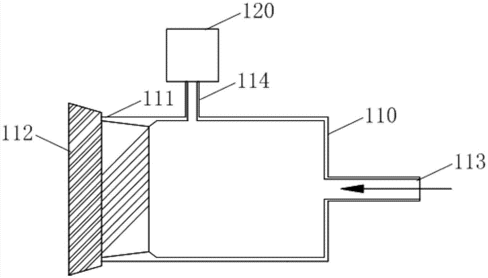
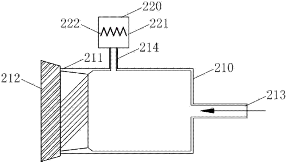
[0033] figure 1 It is a schematic diagram of the heat treatment equipment provided in Embodiment 1 of the present invention. This embodiment is applicable to the case of heat treatment of semiconductor wafers, and the heat treatment equipment can implement the method for heat treatment of wafers.

[0034] A kind of heat treatment equipment provided in t...


PUM


Abstract

The embodiments of the invention disclose a heat treatment device and a wafer treatment method thereof. The heat treatment device comprises a furnace body, a furnace pipe, and a gas treatment unit. The furnace pipe is horizontally arranged inside the furnace body. The mouth of the furnace pipe is equipped with a removable sealing cover, and is used as an inlet via which a wafer is put in. The tail of the furnace pipe is used as a gas transmission port for receiving hydrogen input by an external inflatable device. An exhaust pipe is arranged at a side of the furnace pipe. The gas treatment unit is connected with the exhaust pipe of the furnace pipe, and is used for treating excess gas in the furnace pipe transmitted to the exhaust pipe and discharging the excess gas out of the furnace body. By using the furnace pipe structure and the gas treatment unit of the heat treatment device together, the safety in the process of hydrogen treatment is ensured. The heat treatment device uses a pure hydrogen technology instead of the existing nitrogen technology. The surface state of wafers is improved. The leakage current on the surface of a wafer is reduced. The electrical properties and stability of wafers are improved.

Description

technical field [0001] Embodiments of the present invention relate to the technical field of semiconductor manufacturing, and in particular to a heat treatment device and a method for processing a wafer. Background technique [0002] With the continuous development of semiconductor technology, wafer manufacturing as a basic process has received more and more attention. In the semiconductor wafer manufacturing process, in order to form an ohmic contact between metal and silicon, the wafer must undergo a heat treatment process in an inert gas or reducing gas environment, that is, an alloy process. [0003] The alloy process is an important process in the semiconductor wafer manufacturing process. The process is realized in the diffusion furnace tube, and the process temperature is 400-500 °C. At present, pure nitrogen is generally used as the process gas in the production line. When working, the wafer to be processed is slowly pushed into the furnace tube, and then the gas in...

Claims


Application Information

Patent Timeline
IPC IPC(8): H01L21/67H01L21/324
Inventor 崔严匀季勇
Owner WUXI CHINA RESOURCES HUAJING MICROELECTRONICS
Why Eureka
Try Eureka