Mesa-type photodetector with low surface leakage current and manufacturing method thereof

A technology for photodetectors and manufacturing methods, which is applied in circuits, electrical components, semiconductor devices, etc., can solve problems such as difficulties in passivating sidewall surfaces, and achieve the goals of protecting the surface of the sulfide layer, improving long-term stability, and improving surface adhesion. Effect

Active Publication Date: 2020-11-10
THE 44TH INST OF CHINA ELECTRONICS TECH GROUP CORP
View PDF8 Cites 0 Cited by
  • Summary
  • Abstract
  • Description
  • Claims
  • Application Information

AI Technical Summary

Problems solved by technology

Solve the difficult problem of sidewall surface passivation caused by wet etching of mesa devices

Method used


Image

  • Mesa-type photodetector with low surface leakage current and manufacturing method thereof
  • Mesa-type photodetector with low surface leakage current and manufacturing method thereof
  • Mesa-type photodetector with low surface leakage current and manufacturing method thereof

Examples


Embodiment 1

[0035] The manufacturing method of a low surface leakage current mesa photodetector of the present invention can be realized according to the following scheme:

[0036] (1) Define the mesa etching window, deposit a mask on the top layer of the epitaxial wafer, and open the mesa etching window through the photolithography process;

[0037] (2) The epitaxial wafer is etched into a platform by wet etching, and then the surface is chemically cleaned to remove residual products of the wet etching reaction, surface oxides, and surface impurities.

[0038] (3) Adopt sulfuration process to passivate the side wall surface and reduce its surface state.

[0039] (4) Treat the surface with hexamethyldisilamine (HMDS) to enhance adhesion, and then coat BCB. Under the protection of N2 atmosphere, it is cured by distributed temperature rise.

[0040] (5) Define the P electrode, deposit the metal film by evaporation or sputtering, and form the P electrode pattern after stripping.

[0041] ...

Embodiment 2

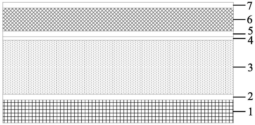
[0049] On the basis of Embodiment 1, this embodiment takes the mesa manufacturing process of avalanche photodiode as a column, and its epitaxial wafer structure is as follows figure 1 Shown includes: N-type InP substrate 1; N-type InP buffer layer 2 with a thickness of 0.1-1 μm and a doping concentration of less than 8×10 17 cm -3 ; Non-doped-InGaAs absorption layer 3, thickness 1-3 μm; N-type InGaAsP gradient layer 4, thickness 0.01-0.1 μm, doping concentration less than or equal to 1×10 17 cm -3 ; The N-type InP charge layer 5 has a thickness of 0.1-0.5 μm and a doping concentration of 5×10 16 ~5×10 17 cm -3 ; InP multiplication layer 6, P-type-InGaAsP contact layer 7, thickness 0.05-0.1 μm, doping concentration greater than 1×10 19 cm -3 .

[0050] Concrete preparation process is as follows:

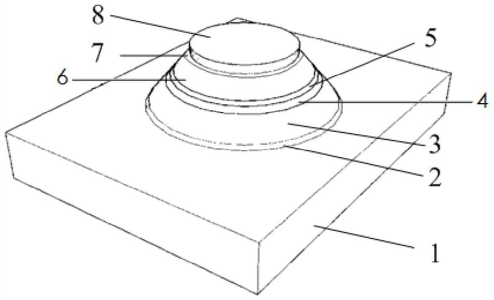
[0051] (11) Using plasma enhanced chemical vapor deposition (PECVD), grow a layer of SiNx / SiO 2 / SiNx composite dielectric film 8 is spin-coated with photoresist through a ph...


PUM

PropertyMeasurementUnit
thicknessaaaaaaaaaa
thicknessaaaaaaaaaa
thicknessaaaaaaaaaa

Abstract

The invention belongs to the technical field of detector chip manufacturing, and specifically relates to a mesa photoelectric detector with low surface leakage current and a manufacturing method thereof. The method comprises the steps of depositing a mask on the top of an epitaxial wafer, and forming mesa etching window through a photoetching process; etching the epitaxial wafer into an epitaxialmesa by adopting wet etching, carrying out chemical cleaning on the surface to remove residual products of the wet etching reaction; passivating the side wall surface of the epitaxial mesa by adoptingvulcanization technology processing to reduce the surface state; processing the side wall surface by using hexamethyldisilazane (HMDS), and then coating benzocyclobutene to form a protective layer; adopting distributed heating and curing under the protection of nitrogen atmosphere; etching part of the protective layer to expose the top of the mesa, depositing a metal film on the upper surface ofa contact layer according to an evaporation of sputtering mode, and forming P-type electrode after peeling; thinning the back, and depositing a reflection reducing film on the back; and manufacturingan N-type electrode by adopting an adhesive tape stripping process. The method solves a problem of difficult side wall surface passivation of the mesa device due to wet etching.

Description

technical field [0001] The invention belongs to the technical field of detector chip manufacture, in particular to a mesa-type photodetector with low surface leakage current and a manufacturing method thereof. Background technique [0002] The performance of semiconductor devices is seriously affected by semiconductor surface effects. In the mesa process, the periodicity of the crystal lattice will be destroyed, and dangling bonds will be generated on the surface of the outermost atoms. These dangling bonds can capture electrons or holes in the body and form a surface depletion layer to increase the surface state. And there are other defects and impurity oxides on the outermost surface. These factors will introduce impurity levels in the forbidden band to generate recombination centers, increase the surface recombination rate, increase the device surface leakage current, and seriously affect the electrical performance of the device. [0003] Mesa-type photodetectors are wid...

Claims


Application Information

Patent Timeline
Patent Type & Authority Patents(China)
IPC IPC(8): H01L31/107H01L31/18H01L31/0216
CPCH01L31/02161H01L31/1075H01L31/1844H01L31/1868
Inventor 张承王立黄晓峰高新江刘逸凡刘海军樊鹏莫才平
Owner THE 44TH INST OF CHINA ELECTRONICS TECH GROUP CORP
Why Eureka
Try Eureka