N type crystalline silicon solar battery and manufacturing method thereof

A technology of a solar cell and a manufacturing method, applied in the field of solar cells, can solve problems such as difficulty in effectively obtaining passivation, and achieve the effects of good passivation effect, reduction of defect density, and reduction of quantity

Active Publication Date: 2012-10-24
YINGLI ENERGY CHINA
View PDF9 Cites 20 Cited by
  • Summary
  • Abstract
  • Description
  • Claims
  • Application Information

AI Technical Summary

Problems solved by technology

[0006] The present invention aims to provide an N-type crystalline silicon solar cell and its manufacturing method to solve the problem that the boron emitter of N-type solar cells is difficult to be effectively passivated in the prior art

Method used


Image

  • N type crystalline silicon solar battery and manufacturing method thereof
  • N type crystalline silicon solar battery and manufacturing method thereof
  • N type crystalline silicon solar battery and manufacturing method thereof

Examples


preparation example Construction

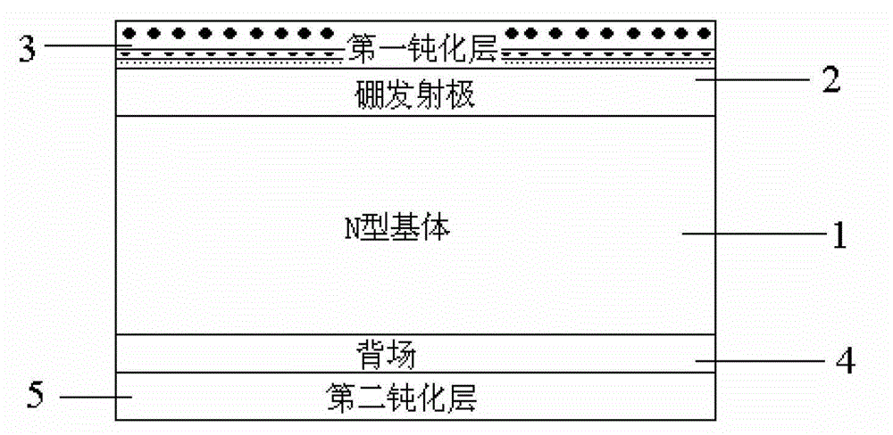
[0031] In order to simplify the preparation method of the aluminum oxide film, preferably step S22 also includes in the process of forming aluminum oxide, after placing the backs of any two N-type substrates prepared with silicon oxide films close to each other, place the silicon oxide film away from the boron emitter Aluminum oxide film is formed on the surface. Since the aluminum oxide film is only formed on the outer surface of the silicon oxide film on the boron emitter, any two N-type substrates are placed back to back when preparing the aluminum oxide film, and the aluminum oxide film is only formed on the front of the N-type substrate , thus simplifying the preparation method of aluminum oxide film.

[0032] Preferably, there is also a silicon nitride film on the outside of the silicon oxide film on the back surface of the N-type substrate of the present invention, and then the manufacturing method also includes separating the silicon oxide film on the surface of the ba...

Embodiment 1

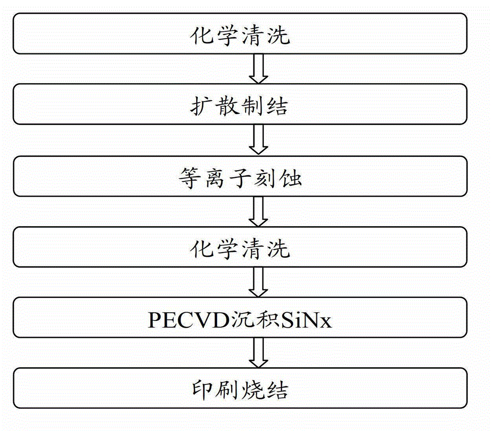
[0036] Preparation of N-type crystalline silicon solar cells:

[0037] A boron emitter is formed on the front of the silicon substrate through boron diffusion to obtain a silicon wafer with a p-n junction. First, a silicon oxide film with a thickness of about 5 nm is prepared on both sides of the silicon wafer with a p-n junction by magnetron sputtering. , in which the silicon oxide film is evenly distributed on the front and back surfaces of the silicon wafer; then, an ultra-thin aluminum oxide film with a thickness of about 3nm is deposited on the silicon oxide film on the boron emitting surface by thermal atomic layer deposition, During the deposition process, the silicon wafers are placed back to back, so that the aluminum oxide film is only deposited on the boron emitter; finally, the PECVD method is used to deposit the silicon nitride film, in which the silicon nitride film is deposited on both the front and back surfaces of the silicon wafer. The thickness of the silico...

Embodiment 2

[0040] A boron emitter is formed on the front of the silicon substrate through boron diffusion to obtain a silicon wafer with a p-n junction. First, a silicon oxide film with a thickness of about 3 nm is prepared on both sides of the silicon wafer with a p-n junction by thermal oxidation. The silicon oxide film is evenly distributed on the front and back surfaces of the silicon wafer; then PECVD is used to deposit aluminum oxide film with a thickness of about 7nm on the silicon oxide film on the boron emission surface; finally, the PECVD method is used to deposit A silicon nitride film is formed, wherein the silicon nitride film is deposited on the front and back surfaces of the silicon wafer, the thickness of the front silicon nitride film is about 80nm, and the thickness of the back silicon nitride film is about 70nm.

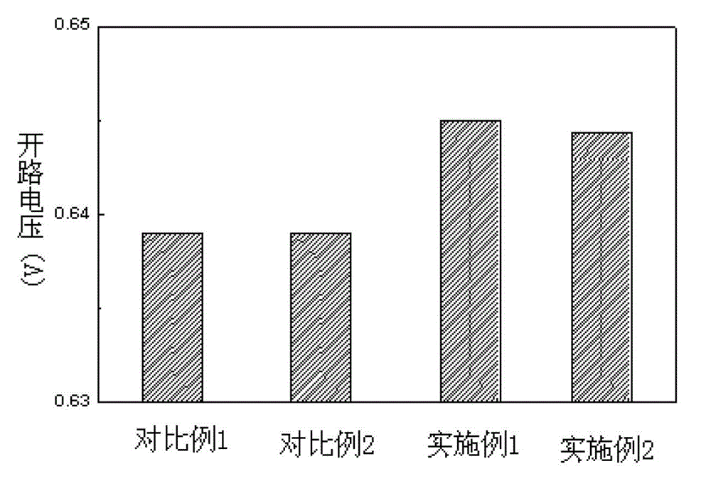
[0041] Test the open circuit voltage of the above-mentioned N-type crystalline silicon solar cell, the results are as attached image 3 shown.


PUM

PropertyMeasurementUnit
thicknessaaaaaaaaaa
thicknessaaaaaaaaaa
thicknessaaaaaaaaaa

Abstract

The invention provides an N type crystalline silicon solar battery and a manufacturing method thereof. The N type crystalline silicon solar battery comprises an N type substrate, a boron emitting electrode and a first passivating layer, wherein the boron emitting electrode is arranged on the front surface of the N type substrate, one surface of the boron emitting electrode, which is far away from the N type substrate, is provided with the first passivating layer, and the first passivating layer is provided with a silicon oxide film, an aluminum oxide film and a silicon nitride film which are arranged from inside to outside. According to the N type crystalline silicon solar battery, the aluminum oxide film on the surface of the boron emitting electrode forms a layer of fixed negative charges at the position of an interface, a few charge carriers which are spread on the surface can be reflected back, the surface recombination rate of photo-generated carriers is reduced, a good field effect pasivating effect is provided, besides, during a sintering process, hydrogen which is enriched in the silicon nitride film can be spread to the position of a SiO2 / Si interface, dangling bonds at the position of the interface are passivated, a good chemical passivating effect is provided, thereby when the silicon nitride film, the aluminum oxide film and the silicon oxide film are utilized to passivate the boron emitting electrode,the field effect passivation and the chemical passivation are provided simultaneously.

Description

technical field [0001] The invention relates to the field of solar cells, in particular to an N-type crystalline silicon solar cell and a manufacturing method thereof. Background technique [0002] Monocrystalline silicon solar cells have been widely used in various fields, and their good stability and mature process flow are the basis for their large-scale application. The production process of monocrystalline silicon solar cells is as follows: figure 1 As shown, the silicon wafer is firstly cleaned, and the surface of the silicon wafer is structured through chemical cleaning; secondly, the cleaned silicon wafer is subjected to diffusion treatment, and the silicon wafer is subjected to a boron diffusion process to form a p-n junction; and then the p-n junction is formed. The silicon wafer undergoes a peripheral etching process to remove the conductive layer formed on the edge of the silicon wafer during the diffusion process; then undergoes a chemical cleaning process to r...

Claims


Application Information

Patent Timeline
Patent Type & Authority Applications(China)
IPC IPC(8): H01L31/0216H01L31/068H01L31/18
CPCH01L31/068H01L31/18H01L31/02167H01L31/0216Y02E10/50Y02E10/547
Inventor 杨德成郎芳李高非胡志岩熊景峰
Owner YINGLI ENERGY CHINA
Why Eureka
Try Eureka