Eureka AIR delivers breakthrough ideas for toughest innovation challenges, trusted by R&D personnel around the world.

Chamber surface passivation method for semi-conductor laser

A laser and semiconductor technology, applied in the direction of semiconductor lasers, lasers, laser parts, etc., can solve the problems of expensive equipment, complex process, instability, etc., and achieve the effect of outstanding passivation effect, simple process method, and improved reliability.

Inactive Publication Date: 2009-03-25
CHANGCHUN UNIV OF SCI & TECH
View PDF0 Cites 22 Cited by
  • Summary
  • Abstract
  • Description
  • Claims
  • Application Information

AI Technical Summary

Problems solved by technology

Although this method can better improve device reliability, it requires high equipment, complicated process and expensive equipment.
In addition, ion beam evaporation of ZnSe and ZnS after ion cleaning on the cavity surface is also a good passivation method. However, ZnSe and ZnS are prone to deliquescence and instability in humid environments, which have certain limitations for the application of lasers in certain aspects. limitation

Method used


Image

  • Chamber surface passivation method for semi-conductor laser

Examples


Embodiment Construction

[0020] 1. After the semiconductor laser is cleaved into strips in the air, it is loaded into a special coating fixture, and then placed in a magnetron sputtering vacuum chamber or an ion beam evaporation vacuum chamber;

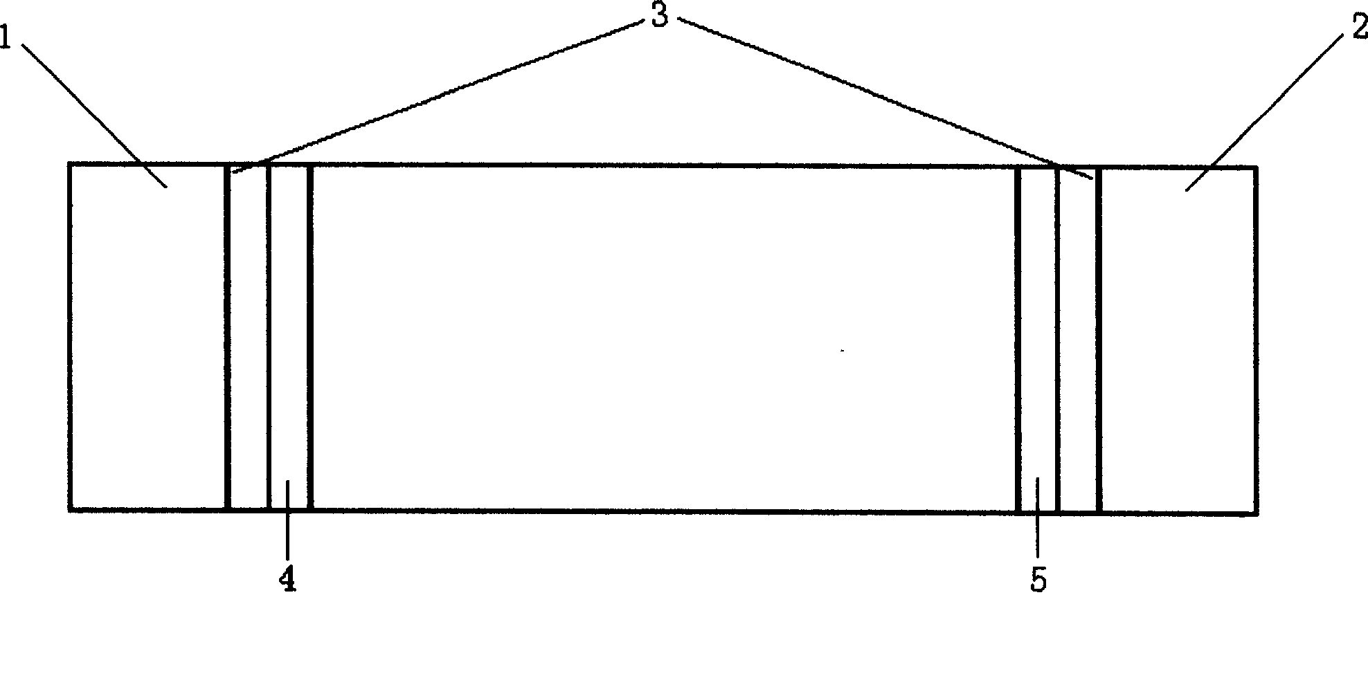
[0021] 2. Hydrogen ion pre-cleaning, that is, bombarding the cleaved cavity surface with hydrogen plasma not less than 105 eV or not less than 50 watts in the electron beam evaporation vacuum chamber or magnetron sputtering vacuum chamber respectively, to remove the oxidation on the cleaved cavity surface At the same time, the hydrogen ions will react with the most electronegative elements within a certain scale on the surface of the cleave cavity surface to generate the hydrogenation of the large electronegative elements. The hydride overflows from the cleaved cavity surface, causing the cavity surface to present positively charged cation characteristics; the hydrogen ion cleaning is carried out on the front cavity surface 4 of the semiconductor laser for 50 ...


PUM


Abstract

A method for passivating a cavity surface of a semiconductor laser belongs to the technical field of the process of a semiconductor photoelectronic device. The known technical difficulties in the field are as follows: the output power is greatly improved, and the reliability of the device maintains a high level. The method for passivating the cavity surface of the semiconductor laser effectively improves the output power and the reliability of the semiconductor laser. The passivation method adopts the cleaning technology for reactive ions of a hydrogen ion and a nitrogen ion in sequence, so that an absorption-free area containing a nitride transition layer is generated on the cleavage cavity surface of the laser, and then a passivation and barrier layer, namely a AIN film coats the transition layer, so as to form a passivation film and then carry out normal coating process. The technical proposal can be applied to the manufacture of various semiconductor laser light sources.

Description

technical field [0001] The invention relates to a method for passivating the cavity surface of a semiconductor laser, which is suitable for narrow and wide semiconductor lasers with multiple wavelengths. Background technique [0002] Semiconductor lasers are core devices in the fields of optical communication, optical pumping, and optical storage. Due to the influence of the interface state, impurity pollution or strain on the cavity surface, the light absorption is enhanced, and the temperature increases sharply, which in turn enhances the light absorption, and it is easy to oxidize and produce defects, which makes the laser energy decay and optical catastrophe. Damage, which is particularly important for the production of high-power optical devices. In order to reduce the influence of these factors and improve the reliability of the laser, the cavity surface of the laser is usually coated. Generally, this coating not only protects the cavity surface, but also plays a rol...

Claims


Application Information

Patent Timeline
IPC IPC(8): H01S5/00C23C14/02C23C14/24C23C14/34C23C14/06
Inventor 乔忠良薄报学高欣胡源么艳萍王玉霞刘春玲李辉卢鹏曲轶马建立
Owner CHANGCHUN UNIV OF SCI & TECH
Why Eureka
Eureka Blog
Learn More