Solar cell provided with amorphous silicon passivation layer and manufacturing method of solar cell
A technology for solar cells and amorphous silicon layers, applied in the field of solar cells, can solve problems such as poor surface passivation effect and poor cell conversion efficiency, and achieve the effect of reducing losses
- Summary
- Abstract
- Description
- Claims
- Application Information
AI Technical Summary
Problems solved by technology
Method used
Image
Examples
Embodiment 1
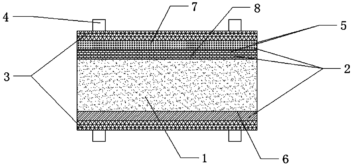
[0038]A solar cell using an amorphous silicon passivation layer, comprising a base layer 1, an amorphous silicon layer 2 arranged on the upper and lower sides of the base layer 1, a transparent conductive oxide layer 3 arranged on the outer surface of the amorphous silicon layer 2, and a The metal electrode 4 on the outer surface of the transparent conductive oxide layer 3; the base layer 1 is a P-type single crystal silicon wafer, and the amorphous silicon layer 2 includes the first N-type silicon wafers arranged in sequence along the upper and lower surfaces of the P-type single crystal silicon wafer. A doped layer 5, a first P-type doped layer 6, the first N-type doped layer 5 includes an N+-a-Si doped layer 7 and an N-c-Si doped layer 8 arranged in sequence from top to bottom, The first P-type doped layer 6 is a P+-a-Si doped layer; a P-type doped and N-type doped amorphous silicon layer is used as a passivation coating to form an N+-a- The step change structure of Si / N-c-...
Embodiment 2
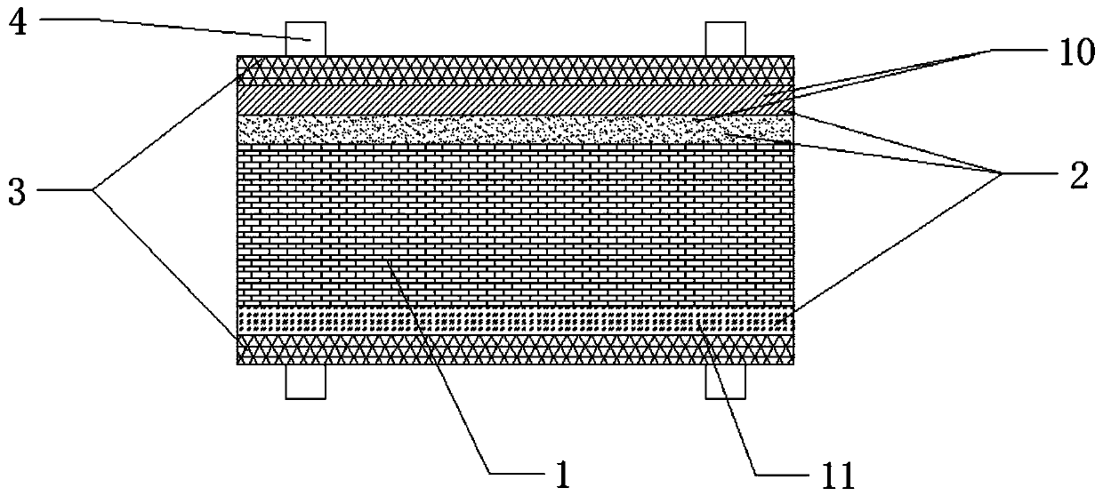
[0040] On the basis of Example 1, the base layer 1 is an N-type monocrystalline silicon wafer, and the amorphous silicon layer 2 includes a second P-type doped layer 10 arranged sequentially along the upper and lower surfaces of the N-type monocrystalline silicon wafer, The second N-type doped layer 11, the second P-type doped layer 10 includes a P+-a-Si doped layer and a P-c-Si doped layer arranged in sequence from top to bottom, and the second N-type doped layer The impurity layer is N+-a-Si doped layer.
Embodiment 3
[0042] On the basis of embodiment 2, both the N+-a-Si doped layer and the P+-a-Si doped layer are hydrogenation-doped amorphous silicon layers.
PUM
 Abstract
Description
Claims
Application Information

