

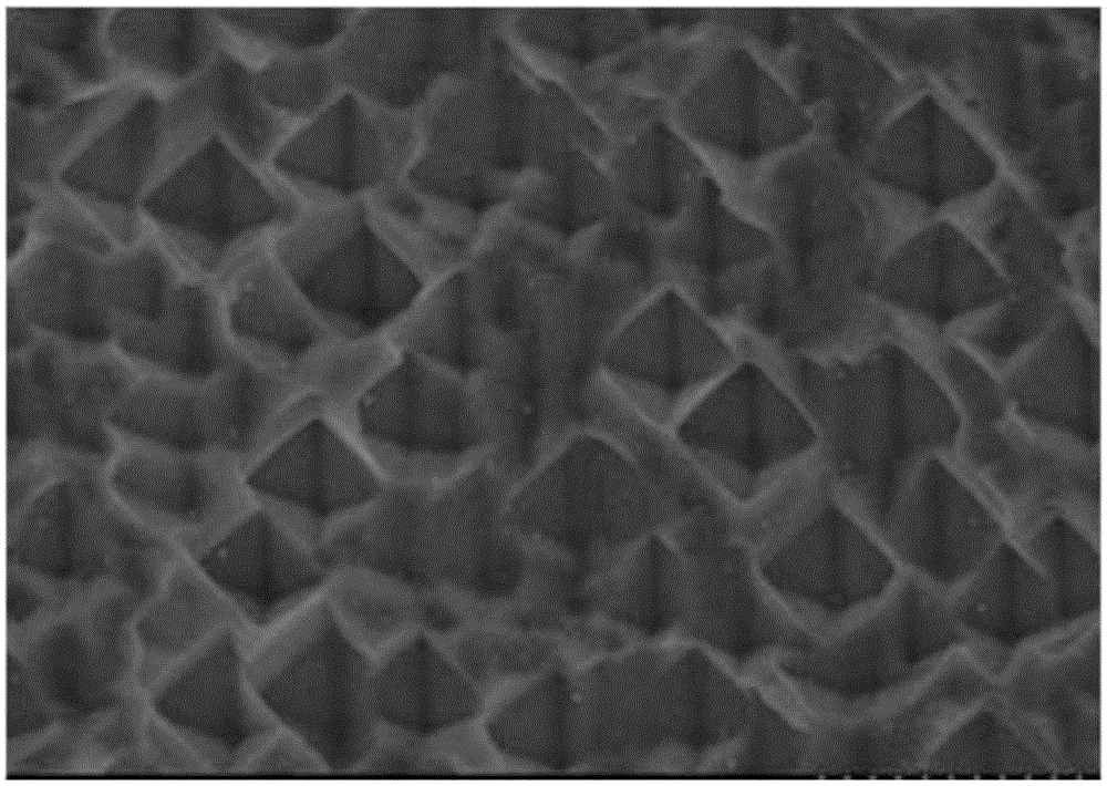
Inverted pyramid structure of polysilicon surface and fabrication method of inverted pyramid structure
An inverted pyramid and polysilicon technology, applied in the field of solar cells, can solve the problems of decreased solar cell efficiency, contamination of impurities on the surface, deep defects, etc., and achieves significant light trapping effect, reduced surface recombination, and easy reflectivity.
- Summary
- Abstract
- Description
- Claims
- Application Information
AI Technical Summary
Problems solved by technology
Method used
Image

Examples
Embodiment 1
[0029] A kind of manufacturing method of polycrystalline surface inverted pyramid structure texture, comprises the following steps:
[0030] Step 1. Select P-type polysilicon material with a size of 156cm*156cm and a thickness of 200mm. Place the polysilicon wafer in hydrofluoric acid and HNO 3 Corrosion in the mixed solution to remove the surface mechanical damage layer;
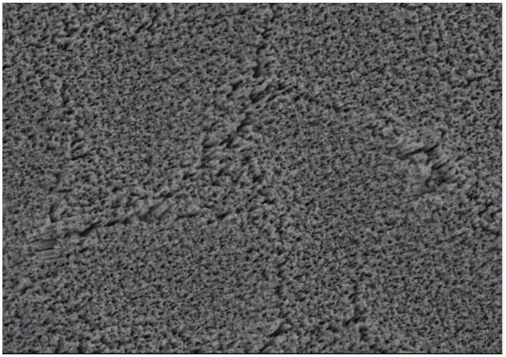
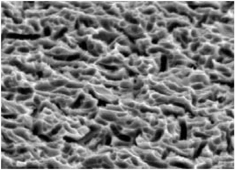
[0031] Step 2. Use metal ion assisted etching method to make black silicon, place the silicon wafer in the mixed solution of hydrofluoric acid and silver nitrate to deposit silver particles for 10s, the reaction temperature is 8°C, and then deposit the deposited polysilicon The sheet was placed in a mixed solution of hydrofluoric acid and hydrogen peroxide for 500s of chemical corrosion, and the reaction temperature was 60°C to obtain a nano-black silicon sample;
[0032] Step 3, then soak the black silicon sample in a mixture of ammonia water, hydrogen peroxide and ethanolamine for 60s at a reaction tempe...
Embodiment 2
[0039] A kind of manufacturing method of polycrystalline surface inverted pyramid structure texture, comprises the following steps:
[0040] Step 1. Select P-type polysilicon material with a size of 156cm*156cm and a thickness of 200mm. Place the polysilicon wafer in hydrofluoric acid and HNO 3 Corrosion in the mixed solution to remove the surface mechanical damage layer;
[0041] Step 2. Use metal ion assisted etching method to make black silicon, place polysilicon wafer in a mixed solution of hydrofluoric acid and silver nitrate to deposit silver particles for 50s, the reaction temperature is 20°C, and then deposit the deposited silicon The sheet was chemically etched in a mixed solution of hydrofluoric acid and hydrogen peroxide for 300s at a reaction temperature of 40°C to obtain a nano-sized black silicon sample;
[0042] Step 3, then soak the black silicon sample in a mixture of ammonia water, hydrogen peroxide and ethanolamine for 300s, and the reaction temperature is ...
Embodiment 3
[0049] A kind of manufacturing method of polycrystalline surface inverted pyramid structure texture, comprises the following steps:
[0050] Step 1. Select P-type polysilicon material with a size of 156cm*156cm and a thickness of 200mm. Place the polysilicon wafer in hydrofluoric acid and HNO 3 Corrosion in the mixed solution to remove the surface mechanical damage layer;
[0051] Step 2. Use metal ion assisted etching method to make black silicon, place polysilicon wafer in a mixed solution of hydrofluoric acid and silver nitrate to deposit silver particles for 50s, the reaction temperature is 20°C, and then deposit the deposited silicon The sheet was chemically etched in a mixed solution of hydrofluoric acid and hydrogen peroxide for 300s at a reaction temperature of 40°C to obtain a nano-sized black silicon sample;
[0052] Step 3, then soak the black silicon sample in a mixture of ammonia water, hydrogen peroxide and ethanolamine for 300s, and the reaction temperature is ...
PUM
 Abstract
Description
Claims
Application Information