

Process for producing semiconductor nanocrystal cores, core-shell, core-buffer-shell, and multiple layer systems in a non-coordinating solvent utilizing in situ surfactant generation
a technology of in situ surfactant and semiconductor nanocrystals, which is applied in the direction of antimony organic compounds, group 3/13 element organic compounds, antimony organic compounds, etc., can solve the problems of affecting the optical properties of the desired iii-v nanocrystal, and properties that have the potential to mask or obscure the optical properties of the desired nanocrystals. , to redu
- Summary
- Abstract
- Description
- Claims
- Application Information
AI Technical Summary
Benefits of technology
Problems solved by technology
Method used
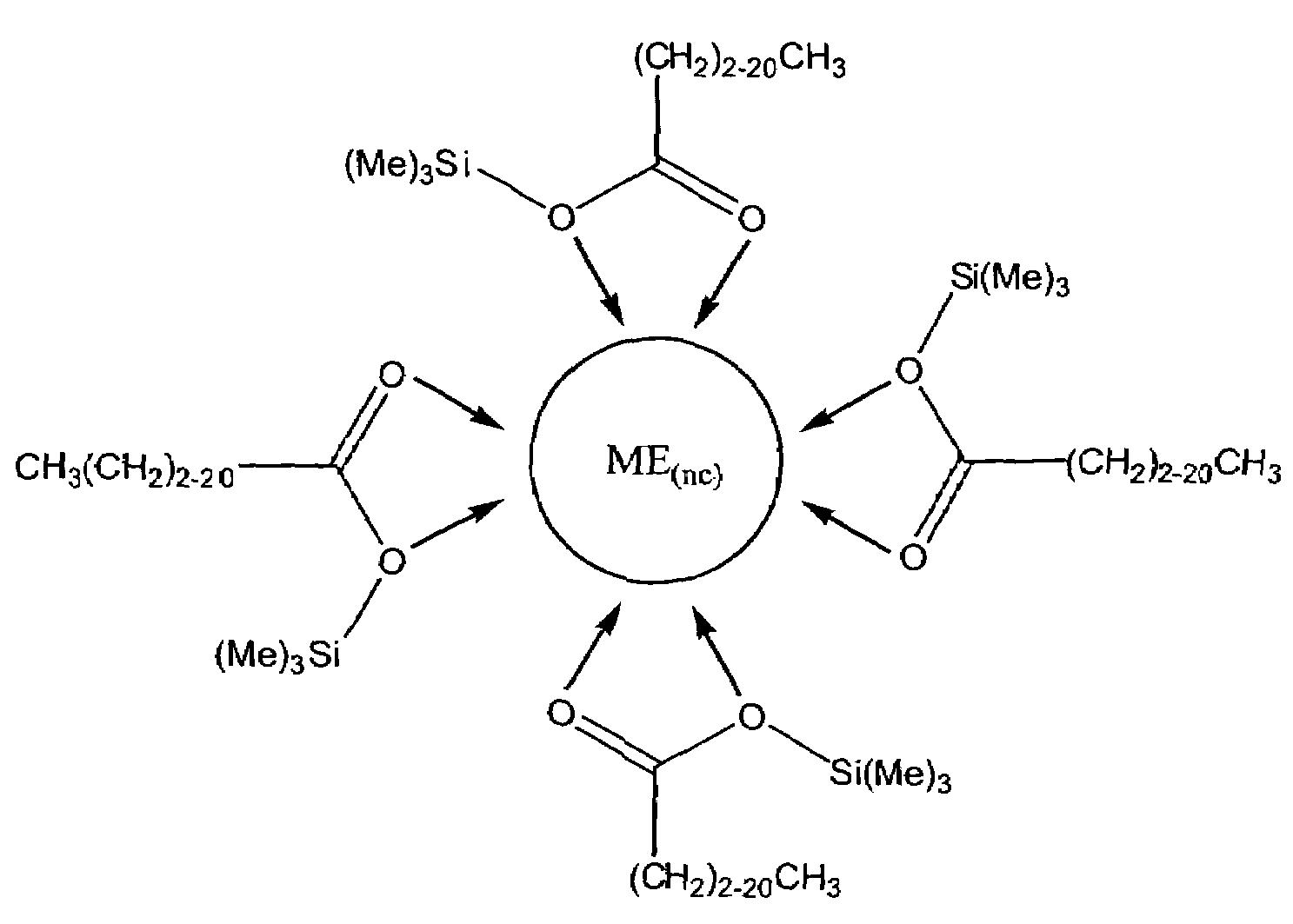
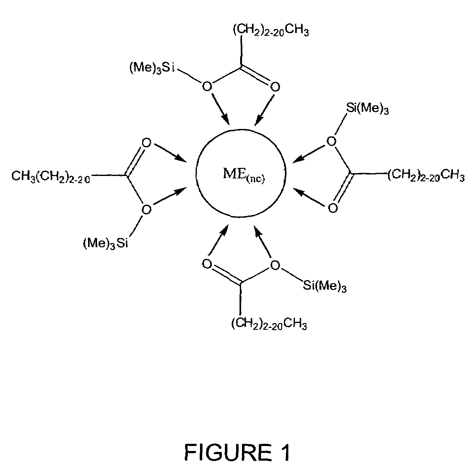
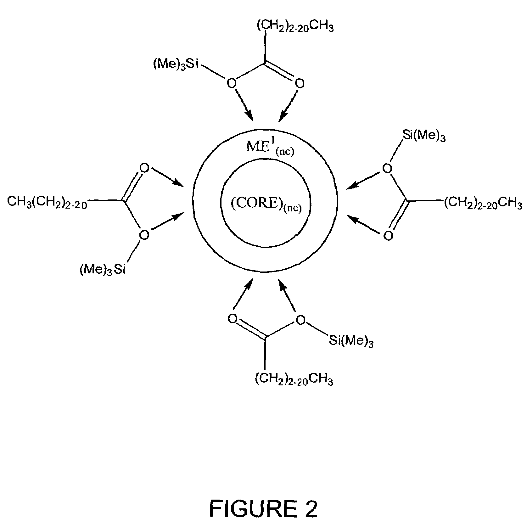
Image

Examples
example 1
Synthesis of Group III Precursors Through Cyclopentadiene Elimination
[0065]The following describes the preparation of very pure Group III precursors which do not contain halide impurities and which do not require the addition of coordinating solvents and / or surfactants for subsequent preparation of semiconductor nanocrystals. Direct synthesis of a series of very pure compounds of the general formula M(ERx)3 is illustrated in Scheme 1.
[0066]
[0067]Even though these complexes might be synthesized directly via the elimination of methane, ethane or neopentane from MMe3, MEt3 or M(CH2CMe3)3, respectively, each subsequent elimination of an alkane molecule requires additional time and subsequently higher temperatures, and the isolation of pure M(ERx)3 complexes becomes very, very difficult. The direct synthesis of M(ERx)3 from In(C5H5)3 and Ga(C5H5)3 was conducted according to Scheme 1 at room temperature in less than 4 hours.
[0068]Table 1 provides examples of compounds of general formula H...
example 2
Synthesis of In(Myristate)3
[0071]A 500 mL three-neck round bottom flask was loaded with 3.4358 grams of In(C5H5)3 (11.08 mmoles), 7.6164 grams of Myristic Acid (33.35 mmoles, 3.01 mol equivalents), a stir bar, and equipped with a glass stopper in one-neck, a medium grain scintered frit which has a 300 mL one-neck round bottom connected via a 24 / 40 ground glass joint and a high-vacuum line adapter. After removal from the glove box, the entire apparatus was connected to the high-vacuum line where approximately 100–150 mL of dry benzene is distilled into the reaction vessel. The benzene was rapidly thawed using warm water and the reaction was stirred for 3–4 hours at room temperature. Next, all of the volatile components were removed by flask to flask distillation and approximately 75–100 mL of dry ether was distilled onto the crude reaction product. Then the sample was filtered through the frit and the volatile ether distilled back onto the product, this process was repeated for thre...
example 3
Synthesis of In(Laurate)3
[0072]The procedure described in the synthesis of In(Myristate)3 was followed, and 2.0968 g In(C5H5)3 (6.76 mmoles) and 4.1642 g Lauric Acid (20.8 mmoles, 3.08 eq) were used. Yield 3.0469 In(Laurate)3, 63.24%. Anal. Calcd for C36H69InO6: C, 60.66; H, 9.76. Found: C, 58.2; H, 10.5. 1H NMR (d6-benzene) T 55° C.: δ 7.15 (benzene), δ 2.59 (br, 2H), δ 1.78 (q, J=7.0 Hz, 2H), δ 1.32 (br, 16H), δ 0.924 (t, J=6.2 Hz, 3H). For comparison Lauric Acid 1H NMR (d6-Benzene) RT: δ 12.72 (br, 1H), δ 7.15 (benzene), δ 2.08 (t, J=7.6 Hz, 2H), δ 1.47 (q, J=7.0 Hz, 2H), δ 1.25–1.13 (br-m, 16H), δ 0.91 (t, J=6.8 Hz, 3H).
PUM
| Property | Measurement | Unit |
|---|---|---|
| temperatures | aaaaa | aaaaa |
| temperatures | aaaaa | aaaaa |
| temperatures | aaaaa | aaaaa |
Abstract
Description
Claims
Application Information