
Method of forming semiconductor device

A semiconductor and device technology, applied in the field of semiconductor device formation, can solve problems such as poor TDDB performance of NMOS metal gate transistors, and achieve the effect of improving TDDB performance

Active Publication Date: 2017-07-14
SEMICON MFG INT (SHANGHAI) CORP
View PDF6 Cites 0 Cited by
  • Summary
  • Abstract
  • Description
  • Claims
  • Application Information

AI Technical Summary

Problems solved by technology

[0011] The problem to be solved by the present invention is: the formation method of existing semiconductor devices can lead to poor TDDB performance of NMOS metal gate transistors

Method used


Image

  • Method of forming semiconductor device
  • Method of forming semiconductor device
  • Method of forming semiconductor device

Examples


no. 1 example

[0065] like Figure 6A and Figure 6B As shown, a substrate 100 is provided, and the substrate 100 includes a PMOS transistor region I and an NMOS transistor region II.

[0066] The substrate 100 may be a common substrate such as a silicon substrate, a silicon germanium substrate, gallium arsenic, and the like. The PMOS transistor region I of the substrate 100 is used to form a PMOS metal gate transistor, and the NMOS transistor region II of the substrate 100 is used to form an NMOS metal gate transistor.

[0067] Then, continue to refer to Figure 6A and Figure 6B As shown, a first dummy gate structure 110 is formed on the PMOS transistor region I of the substrate 100, and a second dummy gate structure 120 is formed on the NMOS transistor region II. The first dummy gate structure 110 includes a first gate dielectric layer 111 and the first dummy gate 112 on the first gate dielectric layer 111, the second dummy gate structure 120 includes the second gate dielectric layer ...

no. 2 example

[0108] The difference between the second embodiment and the first embodiment is that in the second embodiment, there is no metal hard mask layer between the silicon oxide layer and the photoresist layer during the step of removing the first dummy gate.

[0109] In other words, in the second embodiment, the method for removing the first dummy gate includes: forming a silicon oxide layer on the interlayer dielectric layer, the first dummy gate, and the second dummy gate, and forming a silicon oxide layer on the silicon oxide layer. Resist layer; patterning the photoresist layer and the silicon oxide layer to form openings in the photoresist layer and the silicon oxide layer, the opening corresponds to the position of the first dummy gate, and the bottom of the opening exposes the first dummy gate A dummy gate; using the patterned photoresist layer and the patterned silicon oxide layer as a mask to perform dry etching to remove the first dummy gate and form a first dummy gate at t...

no. 3 example

[0112] The difference between the third embodiment and the first embodiment is that in the third embodiment, the plasma treatment step is performed in an ashing machine, and the process parameters of the plasma treatment include: N 2 The flow rate is 500 to 10000sccm (inclusive), the pressure is 100 to 2000mTorr (inclusive), the power supply is 500 to 5000W (inclusive), the time is 10 to 600s (inclusive), and the temperature is 100 to 400°C (inclusive endpoint).


PUM


Abstract

The invention discloses a forming method of a semiconductor device. The device comprises a PMOS (P-channel Metal Oxide Semiconductor) metal gate transistor and an NMOS (N-channel Metal Oxide Semiconductor) metal gate transistor. The method comprises the following steps of providing a substrate, wherein the substrate comprises a PMOS transistor area and an NMOS transistor area; forming a first pseudo-gate structure and a second pseudo-gate structure which are integrated on the PMOS transistor area and the NMOS transistor area respectively, wherein the first pseudo-gate structure comprises a first pseudo-gate, and the second pseudo-gate structure comprises a second pseudo-gate; removing the first pseudo-gate, forming a first metal gate in a first pseudo-gate groove, and then removing the second pseudo-gate by virtue of first dry etching, wherein the first dry etching comprises main etching and over etching, gas adopted for the over etching comprises helium, and a radio frequency power supply for generating plasma in the step of over etching is continuously turned on; forming a second metal gate in a second pseudo-gate groove, wherein the side wall of the first metal gate is in contact with the side wall of the second gate. With the method, the TDDB (Time Dependent Dielectric Breakdown) performance of the NMOS metal gate transistor can be improved.

Description

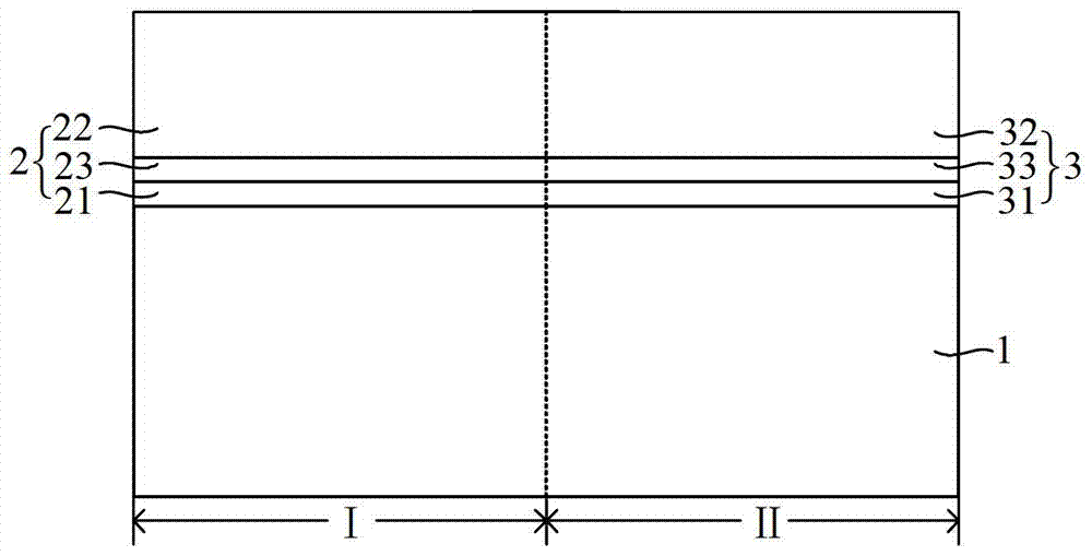
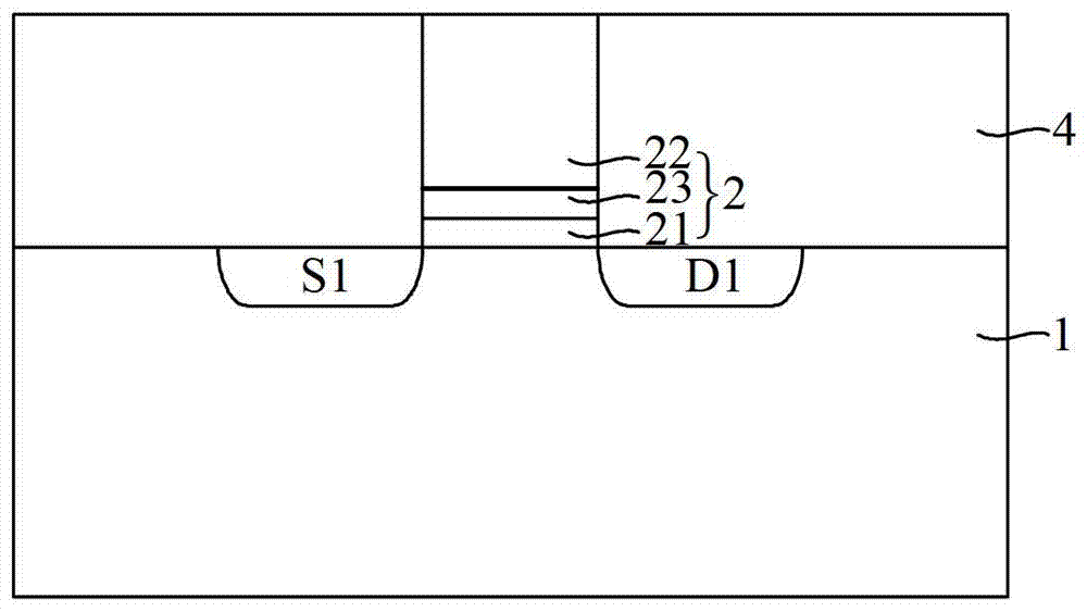
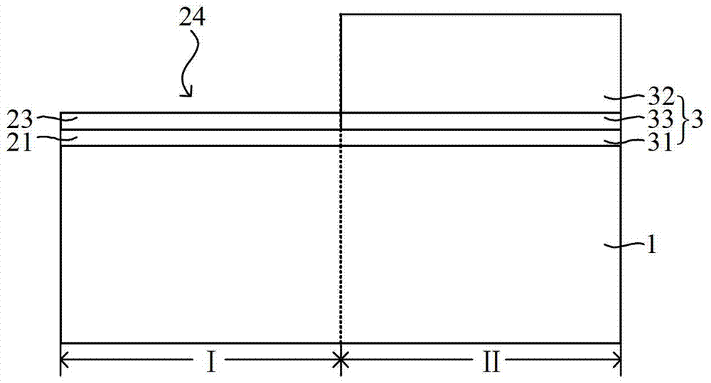
technical field [0001] The invention relates to the technical field of semiconductors, in particular to a method for forming a semiconductor device. Background technique [0002] Most of the logic circuits of existing integrated circuits include such a semiconductor device, the semiconductor device includes a PMOS metal gate transistor and an NMOS metal gate transistor, and the metal gate sidewall of the PMOS metal gate transistor and the metal gate sidewall of the NMOS metal gate transistor metal gate sidewall contacts. The method for forming the semiconductor device includes: [0003] like Figure 1A and Figure 1B As shown, a substrate 1 is provided, and the substrate 1 includes the PMOS transistor region I and the NMOS transistor region II; the first dummy gate structure 2 is formed on the PMOS transistor region I of the substrate 1, and the NMOS transistor region II of the substrate 1 A second dummy gate structure 3 is formed on it, and the first dummy gate structure...

Claims


Application Information

Patent Timeline
Patent Type & Authority Patents(China)
IPC IPC(8): H01L21/8238H01L21/336
CPCH01L21/823828H01L29/401H01L29/4236H01L29/66545
Inventor 张海洋李凤莲尚飞
Owner SEMICON MFG INT (SHANGHAI) CORP
Learn More