
Post Etch Dielectric Film Re-Capping Layer

Active Publication Date: 2010-05-13
TAIWAN SEMICON MFG CO LTD
View PDF15 Cites 5 Cited by
  • Summary
  • Abstract
  • Description
  • Claims
  • Application Information

AI Technical Summary

Benefits of technology

[0020]These and other problems are generally solved or circumvented, and technical advantages are generally achieved, by illustrative embodiments of the present invention which provide methods for re-capping an ARC layer to improve the etch process for vias or trenches, to enhance the TDDB parameter for the devices, to maintain spacing uniformity between vias and between vias and lines, and between lines, and to improve the CD uniformity.
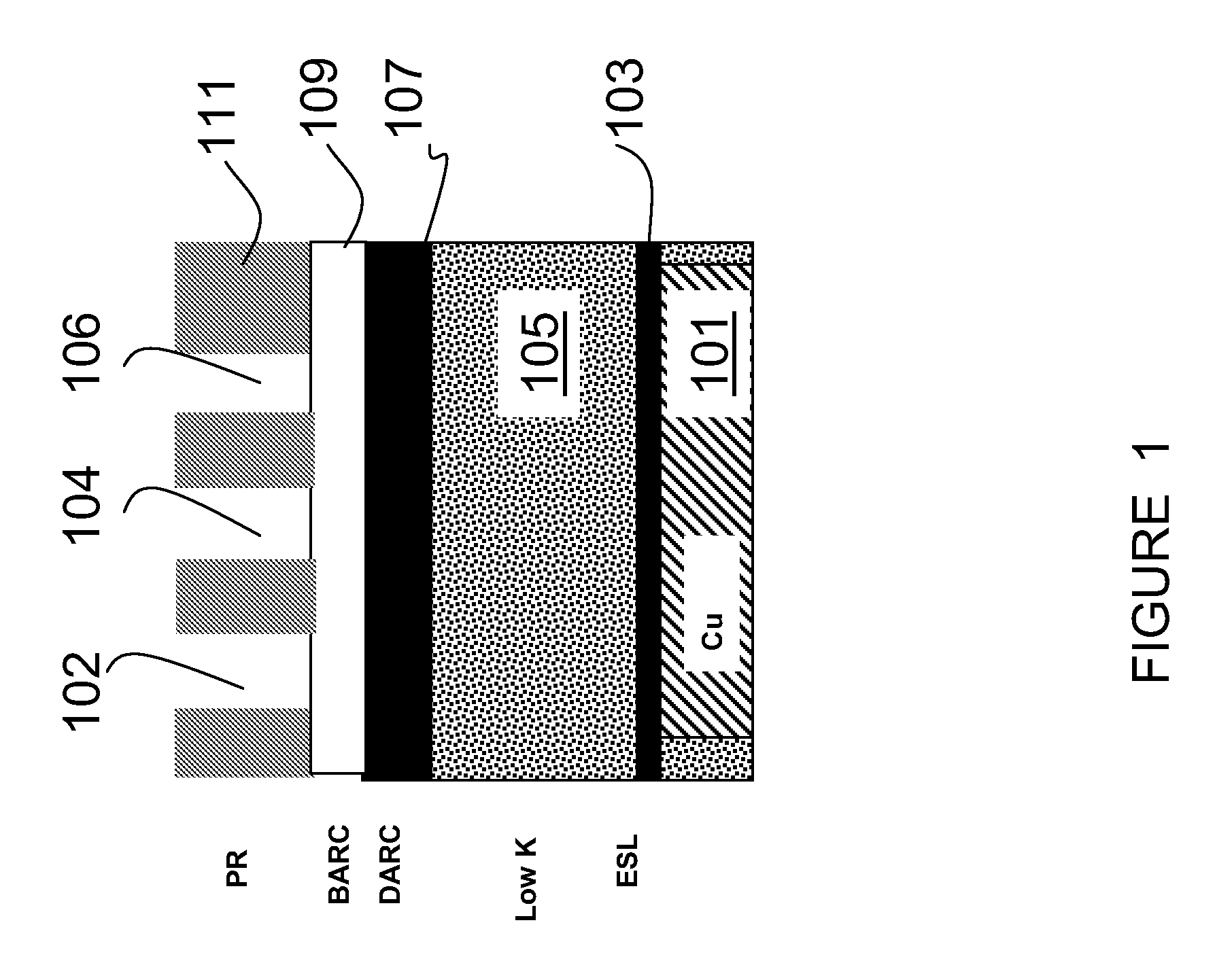
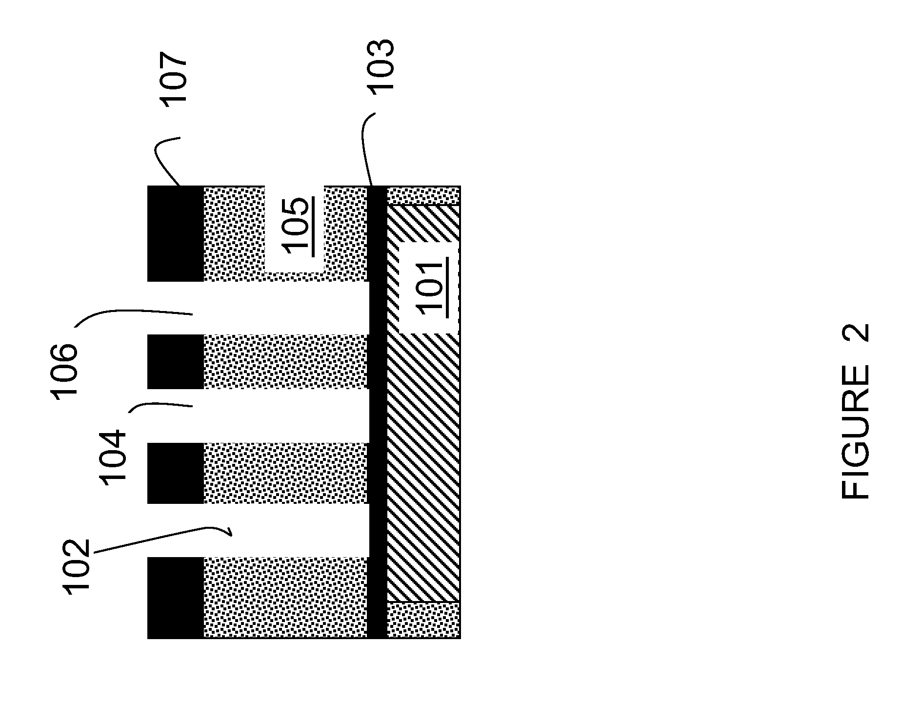
[0021]In accordance with an exemplary embodiment of the present invention, a method for improving the post etch profile of a via or trench through dielectric films is provided, wherein following a first etch process to form the feature, a re-capping deposition of additional film is performed at the remaining top ARC layer. Subsequent etching steps then do not damage the films, the profiles of the etched features are maintained, critical dimension uniformity is achieved, and minimum spacing between features such as vias, vias to line, and line to line, is increased. The time dependent dielectric breakdown (TDDB) parameter is increased.
[0023]Embodiments of the present invention improve CD uniformity, TDDB performance, and spacing. Damage to films in the dielectric layers and the etch stop layer is reduced, the vias achieved maintain a more uniform profile, the methods protect against interface damage or depletion, post etch striation and “bird beak” effects are reduced, and when an extreme low K dielectric is used, the re-capping step provides good adhesion to this layer.
[0024]A further advantage of certain embodiments of the present invention is that the formation of trenches in dielectric films may be improved by recapping the dielectric films following a first etch process to define the feature, then the additional etchback and etch steps will not damage the films defining the trench and the uniformity of the trenches formed will be increased.

Problems solved by technology

The etching process used in the conventional back end of the line (BEOL) metallization and patterning steps will damage film quality.
These process improvements usually involve polymerizing using etch techniques and therefore are subject to etching profile damage.
Critical dimension uniformity (CDU) will also be impacted negatively by these steps.
However the capabilities of the photolithography process remain a bottleneck for advanced semiconductor process technology.
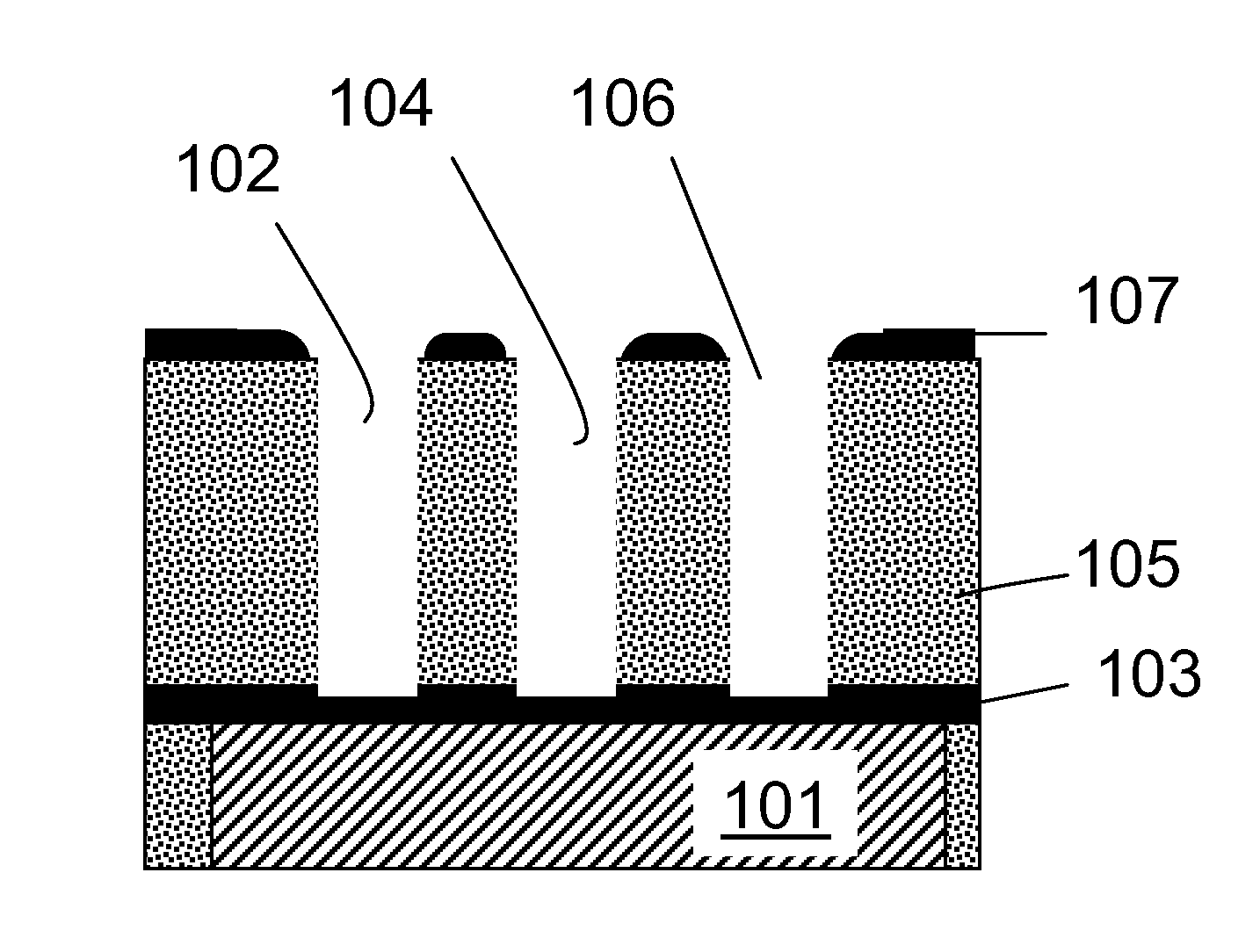
This etch damage causes non uniform spacing, lower minimum spacing between the vias, between vias and lines, and line to line spacing.
In the conventional process, the top critical dimension and the etch stop layer will be damaged by the use of the etch processes.
This minimum spacing design violation is due to the irregular shaped opening at the top of the vias.
The design parameters are not being met in this example, as the etch process is causing the spacing to change.
One disadvantage of the prior art is that the known approaches to improving the TDDB and via shape post etch problems also have disadvantages.
The PR trimming and CD shrinkage of deposition mode in etching processes used in the prior approaches tend to induce additional profile damage.
CD uniformity control will then be worse than if these techniques were not used.
A second disadvantage of the prior art is that the various approaches add complexity to the semiconductor processing and thus tend to increase cost and process time.
In spite of the additional steps, the photolithography processes tend to limit the advance of semiconductor processing.

Method used


Image

  • Post Etch Dielectric Film Re-Capping Layer
  • Post Etch Dielectric Film Re-Capping Layer
  • Post Etch Dielectric Film Re-Capping Layer

Examples


Embodiment Construction

[0039]The making and using of the exemplary embodiments are discussed in detail below. It should be appreciated, however, that the present invention provides many applicable inventive concepts that can be embodied in a wide variety of specific contexts. The specific embodiments discussed are merely illustrative of specific ways to make and use the invention, and do not limit the scope of the invention.

[0040]The present invention will be described with respect to illustrative embodiments in a specific context, namely via formation between metal layers in a copper semiconductor process. The invention may also be applied, however, to other feature formations where etching would otherwise damage films, for example, in forming trenches using etch steps. The methods of the present invention are not limited to a particular process or feature size.

[0041]In FIG. 8, a structure formed using an exemplary method is shown in cross section. This figure shows the result of an additional method ste...


PUM


Abstract

Methods for improving post etch in via or trench formation in semiconductor devices. A preferred embodiment comprises forming a re-capping layer over a dielectric film following an initial etch to form a feature in the dielectric film, followed by additional etch and etch back processing steps. The re-capping method provides protection for underlying films and prevents film damage post etch. Uniform feature profiles are maintained and critical dimension uniformity is obtained by use of the methods of the invention. The time dependent dielectric breakdown performance is increased.

Description

[0001]This application claims the benefit of U.S. Provisional Application No. 61 / 112,584, entitled “Post Etch Dielectric Film Re-Capping Layer,” filed on Nov. 7, 2008, which is incorporated herein by reference.TECHNICAL FIELD[0002]The present invention relates generally to semiconductor processing and methods for improving post etching characteristics of dielectric films for vias or for trench etching. More particularly, in some embodiments, the invention relates to a method for providing a post etching re-capping layer over a dielectric film to improve critical dimension (CD) and time-dependent-dielectric-breakdown (TDDB) characteristics of semiconductor devices produced by the process.BACKGROUND[0003]Generally, semiconductor wafers are produced using photolithography, deposition, etching, damascene and polish steps to form circuitry and conductive layers surrounded by dielectric materials to produce a plurality of integrated circuit dies on a semiconductor wafer.[0004]In conventio...

Claims


Application Information

Patent Timeline
IPC IPC(8): H01L21/311
CPCH01L21/31144H01L2221/1063H01L21/76808
Inventor JENG, SHWANG-MINGWANG, KIN-WENGTSAI, HSIN-YILIN, KENG-CHUKO, CHUNG-CHI
Owner TAIWAN SEMICON MFG CO LTD
Learn More