Group III nitride groove gate normally-closed P-channel HEMT device and manufacturing method thereof
A nitride and groove gate technology, applied in semiconductor/solid-state device manufacturing, semiconductor devices, electrical components, etc., can solve the theoretical limit is still very large, the performance is far from the theoretical value, etching damage and interface state The problem is difficult to solve, etc., to achieve the optimization of normally-off characteristics and conduction characteristics, avoid etching damage, and improve device performance.
- Summary
- Abstract
- Description
- Claims
- Application Information
AI Technical Summary
Problems solved by technology
Method used
Image
Examples
preparation example Construction
[0049] Further, the preparation method may also include:
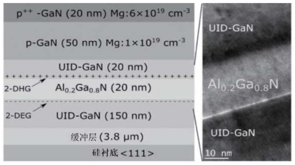
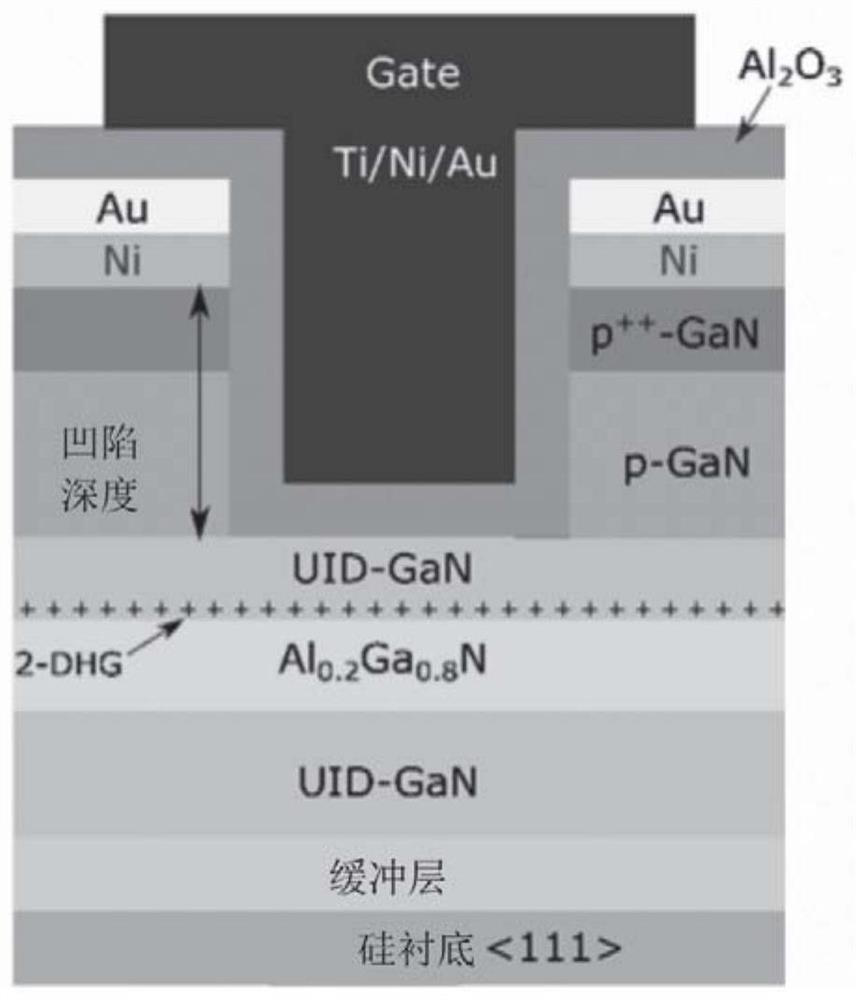
[0050] A mask is set on the third semiconductor, and a local area of the third semiconductor distributed under the gate is removed by band-selective etching, and the etching depth reaches the second semiconductor to form a groove structure;
[0051] A continuous gate dielectric layer is deposited and formed at least on the groove wall of the groove structure.
[0052] Further, the etching method with energy band selectivity includes photo-electrochemical (PEC, Photo-electrochemical) etching technology, but is not limited thereto.
[0053] In some more specific embodiments, the preparation method may also include:
[0054] providing a heterojunction comprising a first semiconductor and a second semiconductor, the second semiconductor being formed on the first semiconductor and having a bandgap narrower than that of the first semiconductor, the heterojunction having 2DHG formed therein;
[0055] disposing a third sem...
Embodiment 1
[0068] Embodiment 1 The polarization effect-based D-2DHG groove gate normally-off HEMT provided in this embodiment includes a GaN buffer layer, an AlGaN barrier layer (i.e. the first semiconductor), a GaN channel layer grown on the substrate in sequence. layer (that is, the second semiconductor) and an InGaN channel layer (that is, the third semiconductor), wherein the GaN channel layer and the AlGaN barrier layer form a first heterojunction, and 2DHG is formed in the first heterojunction, and the GaN channel layer forms a second heterojunction with the InGaN channel layer, and 2DHG is also formed in the second heterojunction. The region corresponding to the gate in the InGaN channel layer is removed to form a groove structure, and the groove structure is arranged in cooperation with the gate structure. The gate structure includes a gate and a gate dielectric layer, the gate is partially disposed in the groove structure, the gate dielectric layer is at least disposed between t...
PUM
 Abstract
Description
Claims
Application Information


