A light splitting device based on the composite structure of graphene and silicon waveguide

A composite structure and light-splitting device technology, applied in the optical field, can solve the problems of low coupling efficiency, non-adjustable frequency band, large size of photonic light-splitting device, etc., and achieve the effects of enhanced interaction, high efficiency, and small input and output loss.

Inactive Publication Date: 2019-07-12
XIAMEN UNIV +1
View PDF3 Cites 0 Cited by
  • Summary
  • Abstract
  • Description
  • Claims
  • Application Information

AI Technical Summary

Problems solved by technology

[0002] Optical fiber connectors and optical splitting devices are the joints of the optical transmission system. Traditional photonic optical splitting devices are large in size and narrow in wavelength range. At the same time, the frequency band is not adjustable and the coupling efficiency is low. This composite structure of graphene and silicon waveguide is proposed and realized by us. A new type of miniature spectroscopic device, which is a new type of spectroscopic method that can be matched with a detector and jointly constitute a miniature spectrometer with simple structure, light weight, high speed and high reliability

Method used


Image

  • A light splitting device based on the composite structure of graphene and silicon waveguide
  • A light splitting device based on the composite structure of graphene and silicon waveguide
  • A light splitting device based on the composite structure of graphene and silicon waveguide

Examples


Embodiment Construction

[0021] The present invention will be further described below in conjunction with the accompanying drawings and specific embodiments.

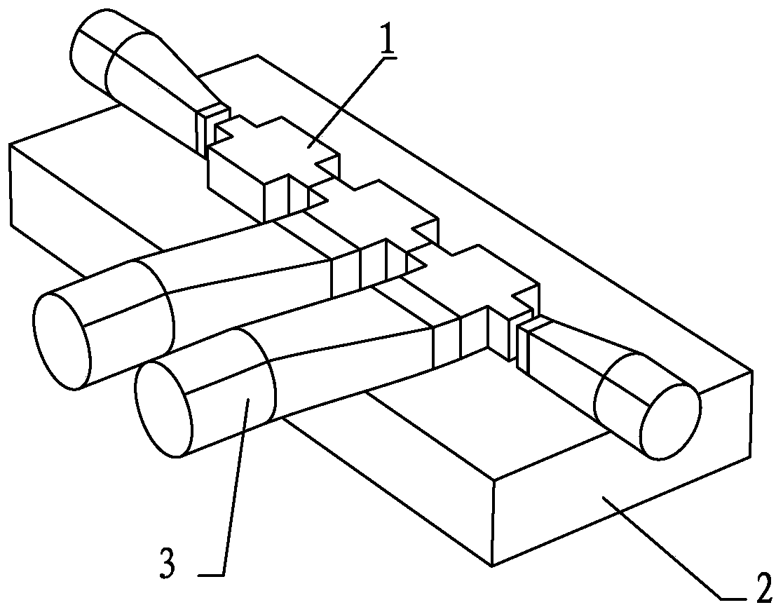
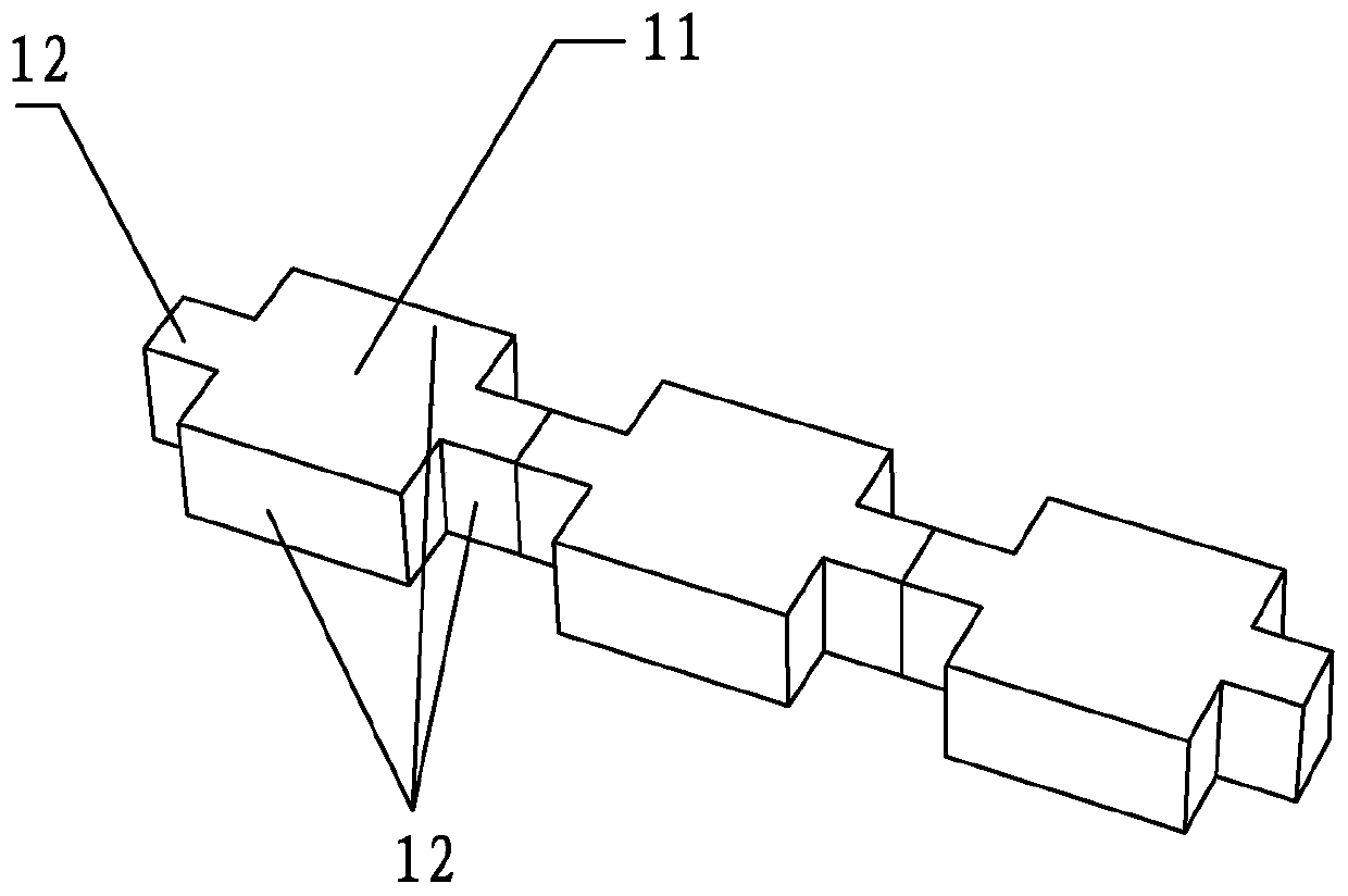
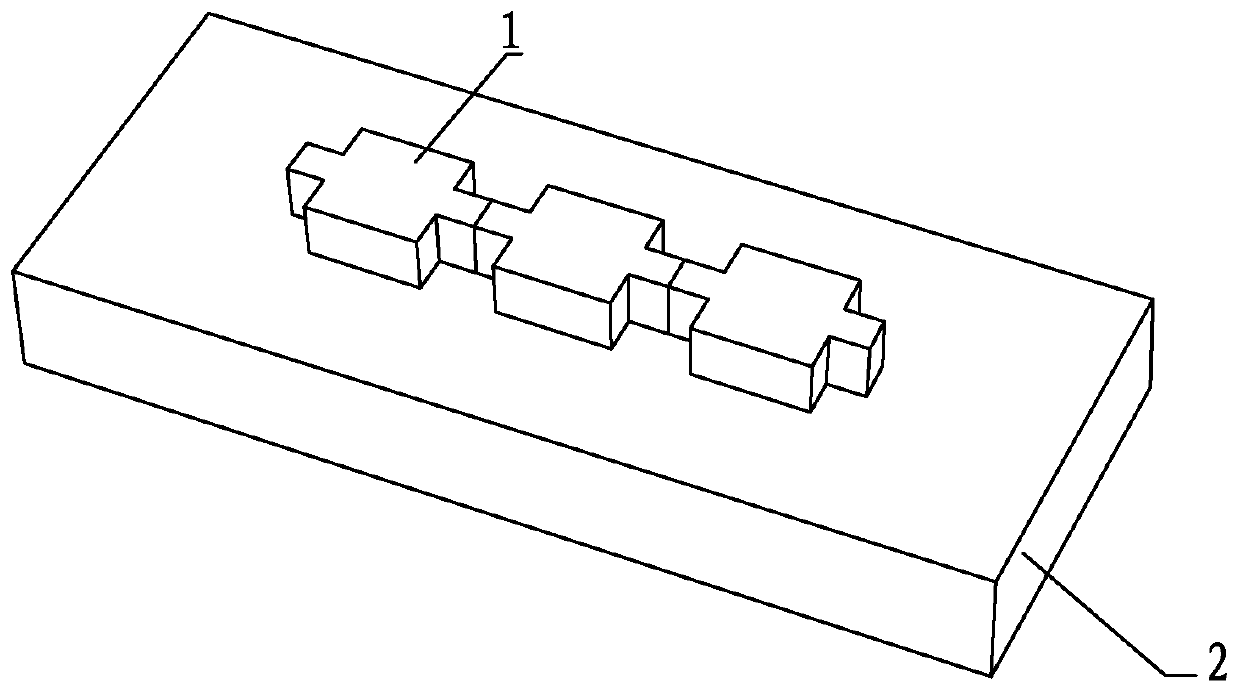
[0022] Such as Figure 1-5 As shown, a light splitting device based on a composite structure of graphene and silicon waveguides includes three silicon waveguides 1 connected in series; the silicon waveguides 1 adopt a cross structure and their upper surfaces are covered with graphene, and each silicon waveguide 1 includes A middle part 11 and input and output ports 12 and 13 arranged at both ends of the middle part 11 along the series direction, the width of the middle part 11 is larger than the width of the input and output ports 12 and 13 to form the cross structure;

[0023] In this embodiment, the specific dimensions of the middle part 11 are: the width of the X axis is 30um, the depth of the Y axis is 30um, and the height of the Z axis is 15um. The specific dimensions of the input and output ports 12 and 13 are: a cuboid with an X-axis wi...


PUM


Abstract

The present invention provides a light-splitting device of a graphene and silicon waveguide-based composite structure. The device comprises a plurality of series-connected silicon waveguides. Each silicon waveguide adopts a cross structure and the graphene is covered on the upper surface of the silicon waveguide. Each silicon waveguide comprises a middle part, an input port and an output port, wherein the input port and the output port are arranged at the two ends of the middle part along the series direction. The width of the middle part is larger than the width of the input port and the width of the output port so as to form the cross structure. The series-connected silicon waveguides are placed on the upper surface of a silicon dioxide substrate. An external electric field is applied on the grapheme on the upper surface of the silicon waveguide at each level. The voltage of the external electric field is sequentially reduced along the series-connected direction. In this way, the graphene and silicon waveguide-based composite structure at each level enables the sequential reduction of the threshold frequency of photons. Meanwhile, the graphene and silicon waveguide-based composite structure at each level converts an absorbed photon into an electric signal, so that the light splitting and the photoelectric conversion are realized. The light-splitting device is simple in structure, light in weight, high in speed and high in reliability.

Description

technical field [0001] The invention relates to the field of optics, in particular to a light splitting device. Background technique [0002] Optical fiber connectors and optical splitting devices are the joints of the optical transmission system. Traditional photonic optical splitting devices are large in size and narrow in wavelength range. At the same time, the frequency band is not adjustable and the coupling efficiency is low. This composite structure of graphene and silicon waveguide is proposed and realized by us. A new type of miniature spectroscopic device is a new type of spectroscopic method that can be matched with a detector to form a micro spectrometer with simple structure, light weight, high speed and high reliability. The structure we designed has the following advantages: Contents of the invention [0003] The main technical problem to be solved by the present invention is to overcome the disadvantages of traditional light splitting devices, and propose ...

Claims


Application Information

Patent Timeline
Patent Type & Authority Patents(China)
IPC IPC(8): G02B6/122G02B6/125G02F1/29
CPCG02B6/122G02B6/125G02F1/29
Inventor 张建寰吴仲永张陈涛
Owner XIAMEN UNIV
Why Eureka
Try Eureka