
Micro mirror surface warp degree detection device and detection method

A detection device and detection method technology, applied in the direction of measuring devices, optical devices, instruments, etc., can solve the problems of high cost of use, low accuracy of warpage measurement, expensive optical profiler equipment, etc., and achieve the calculation method Simple, no-data-processing effects

Inactive Publication Date: 2017-07-14
ANHUI CHINA SCI MW ELECTRONIC TECH CO LTD
View PDF9 Cites 6 Cited by
  • Summary
  • Abstract
  • Description
  • Claims
  • Application Information

AI Technical Summary

Problems solved by technology

However, the optical profiler equipment is expensive, and each test requires strict calibration of the optical path. The cost of use is high, and the accuracy of warpage measurement is not high. Meet the requirements for batch and quantitative testing of micromirrors

Method used


Image

  • Micro mirror surface warp degree detection device and detection method
  • Micro mirror surface warp degree detection device and detection method
  • Micro mirror surface warp degree detection device and detection method

Examples


Embodiment Construction

[0027] The specific implementation of the micromirror surface warping degree detection device and detection method provided by the present invention will be described in detail below in conjunction with the accompanying drawings.

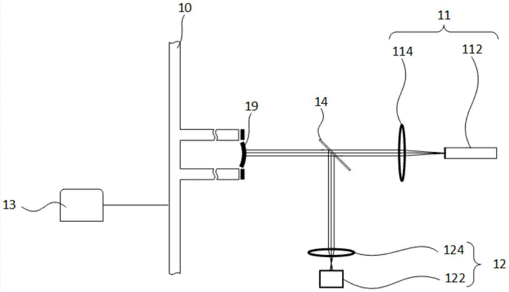
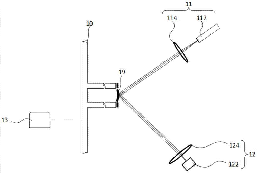
[0028] First, a specific embodiment of the micromirror surface warping degree detection device of the present invention is given in conjunction with the accompanying drawings. attached figure 1 It is a schematic structural diagram of the device described in this specific embodiment, including: a sample stage 10 , an incident light module 11 , a reflected light module 12 and a driving module 13 . attached figure 1 It is only shown as an illustration, and no measurement basis is used. In actual operation, the size of the chip sample to be tested is very small, only on the millimeter level, but the size of the chip sample table is on the centimeter level to ensure that the chip can be placed horizontally. In this specific embodiment, a wafer-level te...


PUM


Abstract

A micro mirror surface warp degree detection device and a detection method are disclosed. The device comprises a sample stage used for placing a micro mirror to be detected, an incident light module used for generating a beam of incident light shining on the surface of the micro mirror to be detected to form an incident spot, a driving module mechanically connected to the sample stage and / or the incident light module and used for driving the sample stage and the incident light module to move relative to each other so as to make the incident spot move on the surface of the micro mirror to be detected, and a reflected light module used for converging the reflected light on the surface of the micro mirror to be detected to form a reflected spot and measuring the displacement of the reflected spot in the process in which the driving module drives the sample stage and the incident light module to move relative to each other. Thus, the warp degree of the surface of the micro mirror to be detected is obtained.

Description

technical field [0001] The invention relates to the field of optical micro-electro-mechanical systems, in particular to a device and a detection method for detecting the degree of warpage of a micromirror surface. Background technique [0002] A micromirror is a MEMS chip integrated with an optical micromirror and a microdrive manufactured based on MEMS process technology. It is the core component of an optical MEMS device, and its mirror size is usually hundreds of microns to thousands of microns. The radius of curvature is the main technical parameter to characterize the surface deformation and warpage of the micromirror. Micromirrors usually use silicon thin films coated with metal materials such as gold or aluminum and optical medium reflection films. The thickness of silicon thin films is generally several microns to tens of microns thick, while the thickness of metal thin films is usually only hundreds of nanometers. Due to the difference in thermal expansion coeffici...

Claims


Application Information

Patent Timeline
IPC IPC(8): G01B11/16G01B11/255
CPCG01B11/16G01B11/255
Inventor 吴亚明翟雷应徐静江火秀
Owner ANHUI CHINA SCI MW ELECTRONIC TECH CO LTD
Features
  • Generate Ideas
  • Intellectual Property
  • Life Sciences
  • Materials
  • Tech Scout
  • Unparalleled Data Quality
  • Higher Quality Content
  • 60% Fewer Hallucinations
Learn More