

Shift register unit and driving method thereof, gate driving circuit and display device
A shift register unit and voltage technology, which is applied to gate drive circuits and display devices, shift register units and their driving fields, can solve the problems affecting the yield rate of display panels, poor GOA driving stability, etc., to avoid mutual competition, The effect of improving poor stability and improving yield
- Summary
- Abstract
- Description
- Claims
- Application Information
AI Technical Summary
Problems solved by technology
Method used
Image

Examples
Embodiment 1
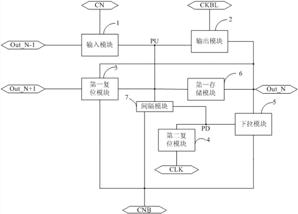
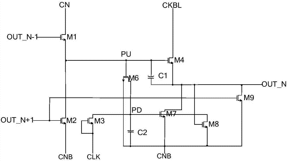
[0050] figure 1 The functional block diagram of the shift register unit provided for Embodiment 1 of the present invention; please refer to figure 1 The shift register unit provided in this embodiment includes an input module 1, an input terminal Out_N-1, an output module 2, an output terminal Out_N, a first clock terminal CKBL, a first reset module 3, a second reset module 4, and a pull-down module 5 , the second clock terminal CLK, the first storage module 6, the pull-up node PU, the pull-down node PD and the interval module 7; wherein:
[0051] The input module 1 is connected to the input terminal Out_N-1, the first voltage terminal CN and the pull-up node PU, and is used to provide the signal of the first voltage terminal CN to the pull-up node when the input terminal Out_N-1 inputs a valid signal PU.
[0052] The output module 2 is connected with the pull-up node PU and the first clock terminal CKBL, and is used for outputting the signal on the first clock terminal CKBL...
Embodiment 2
[0078] Figure 5 For the flowchart of the driving method of the shift register unit provided in Embodiment 2 of the present invention, please refer to Figure 5 , the driving method of the shift register unit includes the following steps:
[0079] S11, input stage: the input terminal inputs a valid signal, and the voltage of the first voltage terminal is provided to the pull-up node to charge the pull-up node; the pull-up node is a valid signal, so that the pull-down node and the second voltage terminal are turned on to charge the pull-down node discharge.
[0080] S12, output stage: the pull-up node is floating, and the first storage module is bootstrapped; the pull-up node is a valid signal so that the signal on the first clock terminal is provided to the output terminal; the pull-down node is kept discharging.
[0081] S13, the first reset stage: a valid signal is input to the reset terminal, so that both the pull-up node and the output terminal are connected to the secon...
Embodiment 3
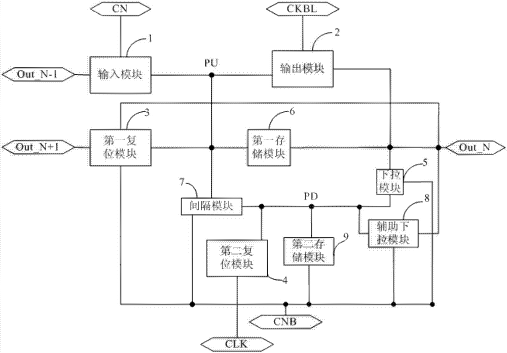
[0086] An embodiment of the present invention further provides a gate driving circuit, which includes a plurality of cascaded shift register units, and the shift register units are the shift register units described in Embodiment 1 above. The composition and driving method of the shift register unit have been described in detail in the above-mentioned embodiment 1 and embodiment 2 respectively. For details, please refer to the content in the above-mentioned embodiment 1 and embodiment 2, and will not be repeated here.
[0087] Wherein, the gate driving circuit may be an N-type gate driving circuit, or a P-type gate driving circuit.
[0088] By using the shift register unit in the gate drive circuit, the stability of the GOA drive can be improved, which is beneficial to improve the yield rate of the display panel.
PUM
 Abstract
Description
Claims
Application Information