Display panel and manufacturing method thereof, display device

A display panel and substrate substrate technology, which is applied in semiconductor/solid-state device manufacturing, electrical components, electric solid-state devices, etc., can solve the problems of poor display uniformity, high cathode resistance, and large voltage drop of OLED display panels, and achieve guaranteed display Uniformity, the effect of reducing pressure drop

Inactive Publication Date: 2017-07-14
BOE TECH GRP CO LTD +1
View PDF8 Cites 22 Cited by
  • Summary
  • Abstract
  • Description
  • Claims
  • Application Information

AI Technical Summary

Problems solved by technology

[0004] However, for large-sized OLED display panels, due to the large area of ​​the cathode, the resistance of the cathode is relatively high. During the driving process of the display device, the voltage drop after the current flows through the cathode is relatively large, making the OLED display panel The display uniformity is poor

Method used


Image

  • Display panel and manufacturing method thereof, display device
  • Display panel and manufacturing method thereof, display device
  • Display panel and manufacturing method thereof, display device

Examples


Embodiment Construction

[0043] In order to make the object, technical solution and advantages of the present invention clearer, the implementation manner of the present invention will be further described in detail below in conjunction with the accompanying drawings.

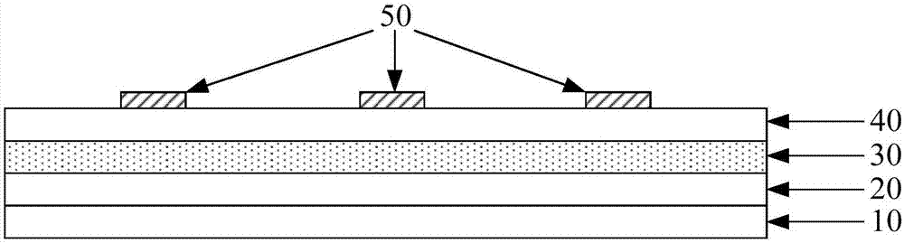
[0044] figure 1 is a schematic structural diagram of a display panel provided by an embodiment of the present invention, refer to figure 1 It can be seen that the display panel may include:

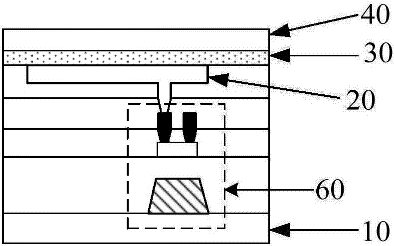
[0045] The base substrate 10 , the first electrode 20 , the light emitting layer 30 and the second electrode 40 are sequentially disposed on the base substrate 10 .

[0046] At least one side of the second electrode 40 is provided with an auxiliary electrode 50, for example, in figure 1 In the shown display panel, the auxiliary electrode 50 is formed on a layer of the second electrode 40 away from the light emitting layer 30 . The orthographic projection of the auxiliary electrode 50 on the base substrate 10 does not overlap with the opening ar...


PUM


Abstract

The invention discloses a display panel, and a manufacturing method thereof, and a display device, and belongs to the technical field of displaying. The display panel comprises a substrate, a first electrode, a light-emitting layer and second electrode which are orderly arranged on the substrate; an auxiliary electrode is arranged on at least one side of the second electrode; the positive projection of the auxiliary electrode on the substrate and an opening region of each pixel are non-overlapping; since the auxiliary electrode and the second electrode are equivalent to a parallel structure, the equivalent resistance of the auxiliary electrode and the second electrode after parallel connection is low, thereby effectively lowering the voltage drop after the current flows through the auxiliary electrode and the second electrode, and then guaranteeing the display uniformity of an OLED display panel. Since the positive projection of the auxiliary electrode on the substrate and the opening region of each pixel unit are non-overlapping, the transmission of the light cannot be shielded; therefore, the structure can be flexibly applied to the OLED display devices in different light-emitting types.

Description

technical field [0001] The present invention relates to the field of display technology, in particular to a display panel, a manufacturing method thereof, and a display device. Background technique [0002] With the development of display technology, Organic Light Emitting Diode (English: Organic Light Emitting Diode; abbreviation: OLED), as a current-type light-emitting device, has become more and more popular due to its characteristics such as self-illumination, fast response, and wide viewing angle. It is widely used in the field of high-performance display. [0003] In the related art, an OLED display panel generally includes an anode, a light emitting layer, a cathode and a color filter layer formed on a base substrate. Wherein, the light emitting layer may specifically include an electron transport layer, an electroluminescence layer and a hole transport layer. When a voltage is applied to the anode and cathode, electrons can migrate from the cathode to the electrolu...

Claims


Application Information

Patent Timeline
Patent Type & Authority Applications(China)
IPC IPC(8): H01L51/52H01L51/56H01L27/32
CPCH10K59/12H10K50/824H10K71/00
Inventor 袁粲徐海侠李永谦
Owner BOE TECH GRP CO LTD
Why Eureka
Try Eureka